Optoelectronic Devices and Properties by Oleg Sergiyenko - HTML preview
Download the book in PDF, ePub, Kindle for a complete version.


6
Optoelectronic Devices and Properties
F8BT/ 9K
F8BT/ 62K
F8BT/ 255K
(a)
Low s
Low ur
u face en
e er
en g
er y
y
Low m
Low o
m l
o ec
e ul
u ar
a w
ei
e ght
g
ht
poly
po me
ly
r
me -ri
- ch
c pha
h
s
pha e
poly
po m
ly er
e -rich
c pha
h
s
pha e
TFB/
3K
100 n
100 m
n
TFB/
(b)
66K
TF
T B
F -
B r
- irch pha
c
se
h pha
F8
F B
8 T
B -
T r
- irch phas
c
e
h phas
100 nm
TFB/
106K
TFB
TF w
B e
w t
e ttitng
n
g l aye
a r
ye
TF
T B
F capp
B
i
capp ng
n l
g ay
a e
y r
e
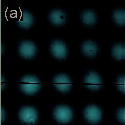
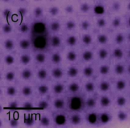
Fig. 1. Left: PL images of F8BT:TFB blend films (100nm, 1:1 by weight) with different MWs
under blue excitation. The bright regions correspond to F8BT-rich phases while the dark
regions TFB-rich phases. Inset: AFM images (20μmX20μm). Right: Proposed cross sections
(a) at least one low MW homopolymers and (b) high MW of both homopolymers
(a) F
a
/
) F 9k
9 :T/3
:T k
(a)
(a
(b)
/3
(b)
(b
(b)
b F/9k:T/
T 66k
10
10
(c) F
(c
/
) F 9k:T
: /1
T 0
/1 6k
)
6
)
(d)
d F/62k:T/
: 3k
(lm/W)
(e)
e F/62k:T/
: 66k
cy
ncy (cd/A
(f)
f F/
F 62k:T/
T 106k
ie
icien
(g) F
g
/
) F 255k:
2
T/
T 3
/ k
r eff
(h) F
h
/
) F 255k:
2
T/
T 6
/ 6k
6
etric effic
owe
(i)
(i F/
F 2
/ 55
5 k:
k T/1
T 06
0 k
m
P
1
1
Photo
1
2
3
4
15
2
3
4
5
Vo
V lt
o age (
age V)
V
Vol
Vo tag
a e (V
g
)
e (V
Fig. 2. EL efficiency-voltage characteristics of LEDs fabricated with F8BT:TFB blend films
with different molecular weights of each copolymer, in (a) cd/A and (b) lm/W
Organic-Organic Semiconductor Interfaces for Molecular Electronic Devices
7
(e) (a)
(a
(b)
10
10
)/A
W)
Lm/
ncy (Cd
cy (en
ficie
ffici
c ef
40
r ee
(d)
etri
30
w
nm 20
om
Po
F8BT:
T TF
T B
10
1
1
Phot
4:1 patt
1 pat er
e ne
n d
e
00
5
10
15
μm
4:1 non-pat
1 non
terne
e
d
rne
1:1 non-pat
1 non
erned
TFB-
B rirch phase
F8BT
F8B -rirch
c phase
phas
1
2
3
4
15
2
3
4
5
Volta
o ge (V)
lta
Volt
Vo ag
a e
g (V
( )
V
Increasi
eas ng
g
Increasi
s ng
300 nm
ng
W
W
TFB
F8B
F8 T
B
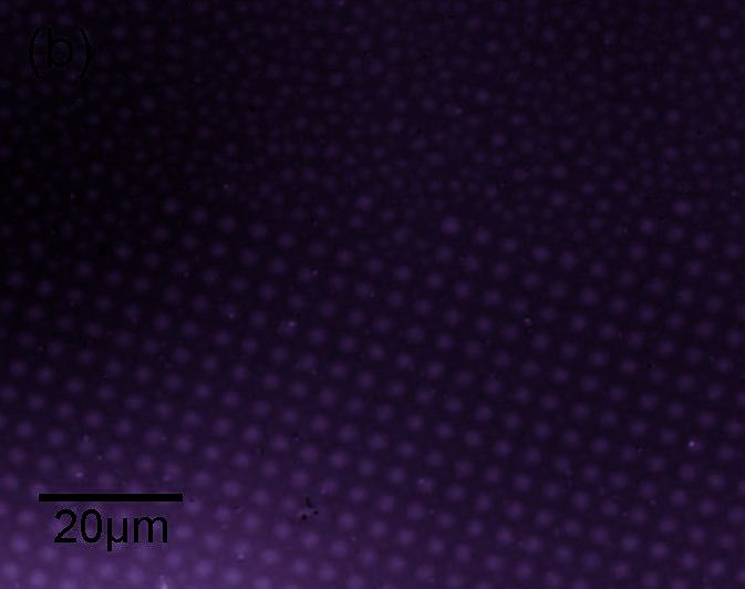
Fig. 3. (a) AFM image (15 μm X 15 μm, on 70 nm height scale) of the patterned F8BT:TFB
blend film. Surface line scan (below) indicates that the height difference between the higher-
lying F8BT-rich and lower-lying TFB-rich phases is ~30 nm. (b) PL image of ~300 nm-thick
patterned F8BT:TFB blend film under blue excitation (2.85 eV). The bright and dark regions
in the PL image correspond to F8BT-rich and TFB-rich phases, respectively. Note the
contrast between the areas with and without the 2D pattern. (c) EL image of the patterned
LED at 7V showing EL from enclosed TFB-rich domains. Differences in brightness between
the TFB-rich domains might be due to thickness variation across the blend film. (d)
Schematic drawing summarizes the proposed cross section of the patterned F8BT:TFB blend
film based on micro-Raman compositional analysis. Both domains show increased purity of
the corresponding polymer nearer to the patterned substrate. (e) EL efficiency-voltage
characteristics of LED fabricated with the patterned blend film expressed in Cd/A and
Lm/W. F8BT:TFB blend devices (4:1 and 1:1 by weight) prepared by spin-coating are
included for comparison
The performance of LEDs fabricated with these blend films is found to be closely related to
the blend thin film morphology, which varies remarkably with the molecular weight of both
polymers (Figure 2). All the devices fabricated with the blend films exhibit sharp turn-on in
both current and luminance at ~2 V. Two distinctive efficiency-voltage characteristics are
observed in these blend devices. First, blend films that exhibit micron-scale lateral phase
separation show high initial efficiencies just after turn-on, but decreases rapidly at high
voltages. Such device characteristics are closely r