Optoelectronic Devices and Properties by Oleg Sergiyenko - HTML preview
Download the book in PDF, ePub, Kindle for a complete version.
OPTOELECTRONIC
DEVICES AND PROPERTIES
Edited by Oleg Sergiyenko
Optoelectronic Devices and Properties
Edited by Oleg Sergiyenko
Published by InTech
Janeza Trdine 9, 51000 Rijeka, Croatia
Copyright © 2011 InTech
All chapters are Open Access articles distributed under the Creative Commons
Non Commercial Share Alike Attribution 3.0 license, which permits to copy,
distribute, transmit, and adapt the work in any medium, so long as the original
work is properly cited. After this work has been published by InTech, authors
have the right to republish it, in whole or part, in any publication of which they
are the author, and to make other personal use of the work. Any republication,
referencing or personal use of the work must explicitly identify the original source.
Statements and opinions expressed in the chapters are these of the individual contributors
and not necessarily those of the editors or publisher. No responsibility is accepted
for the accuracy of information contained in the published articles. The publisher
assumes no responsibility for any damage or injury to persons or property arising out
of the use of any materials, instructions, methods or ideas contained in the book.
Publishing Process Manager Ivana Lorkovic
Technical Editor Teodora Smiljanic
Cover Designer Martina Sirotic
Image Copyright demarcomedia, 2010. Used under license from Shutterstock.com
First published March, 2011
Printed in India
A free online edition of this book is available at www.intechopen.com
Additional hard copies can be obtained from orders@intechweb.org
Optoelectronic Devices and Properties, Edited by Oleg Sergiyenko
p.
cm.
ISBN 978-953-307-204-3
free online editions of InTech
Books and Journals can be found at
www.intechopen.com
Contents
Preface XI
Part 1
New Materials in Optoelectronics 1
Chapter 1
Organic-Organic Semiconductor Interfaces
for Molecular Electronic Devices 3
Ji-Seon Kim and Craig Murphy
Chapter 2
A Study of Adhesion of Silicon Dioxide on
Polymeric Substrates for Optoelectronic Applications 23
E. Amendola, A. Cammarano and D. Acierno
Chapter 3
Organic Semiconductor Based Heterostructures
for Optoelectronic Devices 41
Anca Stanculescu and Florin Stanculescu
Chapter 4
Thin-Film Diamond Phototransistors 73
Linjun Wang, Jian Huang, Ke Tang, Jijun Zhang and Yiben Xia
Chapter 5
Multilayer Approach in Light-Emitting Transistors 89
Gianluca Generali, Stefano Toffanin and Raffaella Capelli
Chapter 6
Effects of Ionizing Radiation
on Optoelectronic Devices 103
V. Th. Tsakiri, A. P. Skountzos, P. H. Yannakopoulos and E. Verrelli
Chapter 7
Identification of Emergent Research Issues:
the Case of Optoelectronic Devices 125
Ivana Roche, Nathalie Vedovotto,
Dominique Besagni, Claire François, Roger Mounet,
Edgar Schiebel and Marianne Hörlesberger
Chapter 8
Synchronous Vapor-Phase Coating
of Conducting Polymers for Flexible
Optoelectronic Applications 151
Keon-Soo Jang and Jae-Do Nam
VI
Contents
Part 2
Nanostructures: Properties and Applications 171
Chapter 9
ZnO Nanostructures for Optoelectronic Applications 173
Ashok K. Sood, Zhong Lin Wang, Dennis L. Polla,
Nibir K. Dhar, Tariq Manzur and A.F.M. Anwar
Chapter 10
Hybrid Optoelectronic and Photovoltaic Materials based
on Silicon Nanocrystals and Conjugated Polymers 197
Vladimir Svrcek
Chapter 11
Synthesis, Self-assembly and Optoelectronic
Properties of Monodisperse ZnO Quantum Dots 215
Ting Mei and Yong Hu
Chapter 12
In-Situ Analysis of Optoelectronic Properties
of Semiconductor Nanostructures and Defects
in Transmission Electron Microscopes 241
Yutaka Ohno, Ichiro Yonenega and Seiji Takeda
Chapter 13
Investigating Optoelectronic Properties of the NbN
Superconducting Nanowire Single Photon Detector 263
Zhizhong Yan
Chapter 14
Band Structure and Magneto- Transport Properties
in II-VI Nanostructures Semiconductors -
Application to Infrared Detector Superlattices 283
Abdelhakim Nafidi
Part 3
Optoelectronic Measurements in Spatial Domain 305
Chapter 15
3D Body & Medical Scanners’ Technologies:
Methodology and Spatial Discriminations 307
Julio C. Rodríguez-Quiñonez, Oleg Sergiyenko, Vera Tyrsa,
Luís C. Básaca-Preciado, Moisés Rivas-Lopez,
Daniel Hernández-Balbuena and Mario Peña-Cabrera
Chapter 16
Research and Development
of the Passive Optoelectronic Rangefinder 323
Vladimir Cech and Jiri Jevicky
Chapter 17
Methods and Devices of Processing Signals
of Optoelectronic Position Transducers 349
Zbigniew Szcześniak and Adam Szcześniak
Chapter 18
Optoelectronic Measurements in Science and Innovative
Industrial Technologies 373
Vladimir G. Meledin
Contents
VII
Part 4
Optoelectronic Measurements in Frequency Domain 399
Chapter 19
Optoelectronic Oscillators 401
Patrice Salzenstein
Chapter 20
Statistical Tools and Optoelectronic
Measuring Instruments 411
Ionel Sabin and Ionel Ioana
Part 5
Physical Modeling and Simulations
of Optoelectronic Devices 431
Chapter 21
Advanced Numerical Simulation
of Organic Light-emitting Devices 433
Beat Ruhstaller, Evelyne Knapp, Benjamin Perucco,
Nils Reinke, Daniele Rezzonico and Felix Müller
Chapter 22
Design and Simulation of Time-Pulse Coded
Optoelectronic Neural Elements and Devices 459
Vladimir G. Krasilenko, Aleksandr I. Nikolskyy
and Alexander A. Lazarev
Chapter 23
Optical and Electrical Spectrum Analysis
of Optoelectronic Devices 501
Ning Hua Zhu, Wei Chen, Wei Li, Li Xian Wang,
Xiao Qiong Qi and Bang Hong Zhang
Chapter 24
Bistable Photoconduction in Semiconductors 527
Stefano Lagomarsino
Part 6
Laser Devices and Methods 547
Chapter 25
Electromechanical 3D Optoelectronic Scanners:
Resolution Constraints
and Possible Ways of Improvement 549
Oleg Sergiyenko, Vera Tyrsa, Luís C. Basaca-Preciado,
Julio C. Rodríguez-Quiñones, Wilmar Hernández,
Juan I. Nieto-Hipólito, Moisés Rivas Lopez and Oleg Starostenko
Chapter 26
Employment of Pulsed-Laser Deposition
for Optoelectronic Device Fabrication 583
Ullrich Bruno
Chapter 27
Optical Spectral Structure
and Frequency Coherence 603
Ning Hua Zhu, Wei Li, Jian Hong Ke,
Hong Guang Zhang, Jiang Wei Man and Jian Guo Liu
VIII
Contents
Part 7
Optical Communications 629
Chapter 28
Optoelectronic Chaotic Circuits 631
M.P. Hanias, H.E. Nistazakis and G.S. Tombras
Chapter 29
Optoelectronic Feedback in Semiconductor
Light Sources: Optimization of Network
Components for Synchronization 651
Sora F. Abdalah, Marzena Ciszak, Francesco Marino,
Kais Al-Naimee, Riccardo Meucci and F. Tito Arecchi
Preface
Optoelectronic devices impact many areas of society, from simple household appli-
ances and multimedia systems to communications, computing, spatial scanning, opti-
cal monitoring, 3D measurements and medical instruments. This is the most complete
book about optoelectromechanic systems and semiconductor optoelectronic devices; it
provides an accessible, well-organized overview of optoelectronic devices and proper-
ties that emphasizes basic principles. Coverage combines an optional review from key
concepts such as properties of compound semiconductors, semiconductor statistics,
carrier transport properties, optical processes, etc., up to gradual progress through
more advanced topics. This book includes the recent developments in the fi eld, empha-
sizes fundamental concepts and analytical techniques, rather than a comprehensive
coverage of diff erent devices, so readers can apply them to all current, and even future,
devices.
In this book are introduced novel materials and physico-chemical phenomena useful
for new tasks solution. It discusses important properties for diff erent types of applica-
tion, such as analog or digital links, the formation and analysis of optical waveguides;
channel waveguide components; guided wave interactions; electrooptical eff ects; time
dependence, bandwidth and electrical circuits.
Given the demand for ever more compact and powerful systems, there is growing in-
terest in the development of nanoscale devices that could enable new functions and
greatly enhanced performance. Semiconductor nanowires are emerging as a powerful
class of materials that, through controlled growth and organization, are opening up
substantial opportunities for novel photonic and electronic nanodevices.
Also progress in the area of nanowires growth is reviewed, as well as the fundamental
electronic and optoelectronic properties of semiconductor nanowires and nanowire
heterostructures, as well as strategies for and emerging results demonstrating their
promise for nanoscale device arrays. Nanowires made could be ideal building blocks
for making nano-optoelectronic devices; the nanowires sometimes show periodic de-
fect structures along their lengths, which may be crucial for determining the optical
properties of the material, so nanostructures may lead to further novel properties and
promising applications such as point defects and stacking faults.
A signifi cant part of optoelectronic methods are contributed in various geometric mea-
surements like rangefi nders, various 2D and 3D vision systems, with several applica-
tions in robot navigation, structural health monitoring, medical and body scanners.
XII
Preface
Optoelectronic measurements are still among of the most att ractive tools in a both spatial and
frequency domains.
Independently a review of a wide range of optical fi ber communication and optoelectronic
systems is presented. In such networks, the electrical and the optical characteristics of guided-
wave devices have a profound eff ect on the system design and overall performance. This book
generally combines both the optical and electrical behavior of optoelectronic devices so that
the interwoven properties, including interconnections to external components. It also shows
the impact of material properties on various optoelectronic devices, and emphasizes the impor-
tance of time-dependent interactions between electrical and optical signals. It provides the key
concepts and analytical techniques that readers can apply to current and future devices.
This is an ideal reference for graduate students and researchers in electrical engineering and
applied physics departments, as well as practitioners in the optoelectronics industry.
Oleg Sergiyenko
The Engineering Institute,
Autonomous University of Baja California,
Mexicali, Mexico
Part 1
New Materials in Optoelectronics
1
Organic-Organic Semiconductor Interfaces for
Molecular Electronic Devices
Ji-Seon Kim1 and Craig Murphy2
1Department of Physics & Centre for Plastic Electronics, Imperial College London,
2National Physical Laboratory (NPL)
United Kingdom
1. Introduction
Molecular (Plastic) electronics encompasses the materials science, chemistry and physics of
molecular electronic materials and the application of such materials to displays, lighting,
flexible thin film electronics, solar energy conversion and sensors. The field is a growth area,
nationally and globally, evidenced by the rapidly expanding organic display and printed
electronics industries. Organic semiconductors combine the semiconductor properties
traditionally associated with inorganic materials with the more desirable properties of
plastics. Moreover, the organic syntheses of these materials allow for great flexibility in the
tuning of their electronic and optical properties. By combining these properties, organic
semiconductors such as conjugated polymers have been demonstrated as the active material
in light-emitting diodes (LEDs), transistors, and photovoltaic (PV) cells. Furthermore, these
conjugated polymers provide a new way of looking at many of the broad fundamental
scientific issues related to using molecules for electronics. A great deal of the physics which
governs the behaviour of molecules for electronics occurs at the organic-organic interfaces
(heterojunctions). For example, the nature of organic interfaces determines the fate of
excitons to be either stabilised (for efficient LEDs) or destabilised (for efficient PV cells) at
the interfaces. Therefore, by selecting semiconductors with proper band-edge offsets
between their conduction and valence bands, different device characteristics can be readily
achieved. While significant progress has been made in developing the materials and high
performance organic devices, many fundamental aspects of organic-organic semiconductor
interfaces remain to be understood. In particular, fundamental understanding of the
correlation between nanostructures and interfaces of organic semiconductors in thin films
and multilayers and associated device performance still remain to be fully explored. In this
Chapter, we will introduce how to control and characterise various length-scale organic-
organic interfaces facilitating the rational design of materials, device architectures and
fabrication methods via increased understanding of fundamental properties of organic-
organic interfaces and their modification due to processing. In particular, we will address
the distinctive optoelectronic and charge transport properties which have been observed
across different organic-organic interfaces depending on their length-scale (micron-scale in
the blends down to molecular-scale in the copolymers) and nature (interchain vs intrachain),
providing the deeper understanding of organic interfaces and their vital roles in various
optoelectronic devices. The key advances in organic semiconductor interfaces achieved so
4
Optoelectronic Devices and Properties
far will provide important insight into a design rule of organic semiconductors which is
essential for future development in molecular electronic devices.
2. The main aim and contents of this chapter
This chapter aims to review fundamental scientific issues related to using molecules for
electronics down to the single-molecule scale by studying a range of well-controlled
organic-organic interfaces, with a particular focus on their role on electronic structures and
electronic processes of organic semiconductors and their devices. Specific topics were:
1. Control and characterisation of various length-scale organic interfaces (Section 3)
2. Photophysical dynamics of electronic species at the organic interfaces (Section 4)
3. Electronic processes of charge carriers across the organic interfaces (Section 5)
4. Charge-carrier operational dynamics across the organic interfaces (Section 6)
3. Control and characterisation of various length-scale organic interfaces
3.1 Interfaces controlled by polymer molecular weight variation
Polymer molecular weight (MW) (i.e. chain length) variation was used as a tool to control
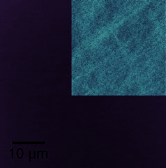
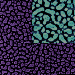
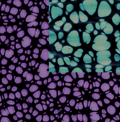
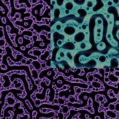
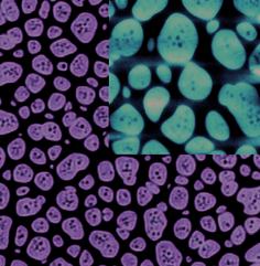
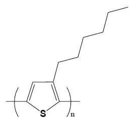
the phase separation laterally and/or vertically in blend films (Yim et al., 2010). The
conjugated polymers studied are poly(9,9-di- n-octylfluorene- alt-benzothiadiazole) F8BT (Mn
= 9 - 255 kg/mol) and poly(9,9-di- n-octylfluorene- alt-(1,4-phenylene-((4- sec-butylphenyl)
imino)-1,4-phenylene) TFB (Mn = 3 - 102 kg/mol) (Chemical structures in Table 1). Micron-
scale lateral phase separation is observed in blend films that consist of high MW of both
F8BT and TFB (Mn > 60 kg/mol), in which domain sizes increase with MW of each
homopolymer. For these blend films, the micro-Raman spectroscopy study indicates that the
higher-lying domains are F8BT-rich and the lower-lying domains are TFB-rich. In contrast,
the blend films that consist of at least one low MW homopolymer (Mn < 10 kg/mol) show
relatively smooth surface with sub-micron or no measurable lateral phase separation.
Using the surface-sensitive X–ray photoelectron spectroscopy (XPS) technique, it is observed
first that, for blend films that consist of at least one low MW polymer (Mn < 10 kg/mol),
there is a significant enrichment of the short polymer chains at the film-air interface. This
reveals that the vertical phase segregation at the film-air interface is driven by the contrast of
MW between the two homopolymers. On the other hand, for blend films that show micron-
scale lateral phase separation, the film-air interface is always enriched with TFB, suggesting
the presence of TFB capping layer apart from the exposed TFB-rich domains. Second, for all
the blend films at the film-substrate interface, there is an enrichment of the lower surface
energy material (TFB). The extent of TFB enrichment is found to increase with the MW of
both polymers, possibly due to increased thickness or purity of the TFB wetting layer in
these blend films. These observations suggest that surface energy contrast (as oppose to MW
contrast) might be the dominant driving force in determining the vertical phase segregation
at the film-substrate interface. Based on the morphological and compositional analyses of
these blend films, we proposed two different models of the final phase separated structures
(Fig 1a and 1b) for blend films without and with micron-scale lateral phase separation,
respectively.
For the blend films with no visible lateral phase separation (in which a large MW contrast
exists between the two homopolymers), the film-air interface is enriched with the low MW
polymer, while the film-substrate interface is always enriched with the lower surface energy
Organic-Organic Semiconductor Interfaces for Molecular Electronic Devices
5
polymer TFB. For the blend films with obvious micron-scale lateral phase separated
structures, additional nanoscale vertical phase segregation also occurs resulting in a
continuous TFB wetting layer at the film-substrate interface and a discontinuous TFB
capping layer at the film-air interface (aKim et al., 2004). These remarkably different lateral
and vertical phase separation observed in the F8BT:TFB blend films has important
implications on LED performance.
Material
Chemical Structure
HOMO
PL
[eV] efficiency
P3HT
-4.8
0.1
0[a]
PFB
N
N
-5.1
0.65
n
0[a]
C8
C H
8 17
H
C8
C H
8 17
H
0.35[b]
TFB
N
-5.3
0.4
n
C8H17
C8H17
0.05[a]
0.1[b]
F8BT
-5.9
0.6
n
N
N
0.05[a]
C8H17
C8H17
S
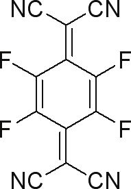
F4-TCNQ
-5.2[c]
-
Table 1. Chemical structures and optoelectronic properties of conjugated polymers and
F4TCNQ. [a] PL efficiency of 5 % F4TCNQ-doped polymer, [b] PL efficiency of 5 %
F4TCNQ-doped polymer after annealing (N2 environment, 200 ºC, 1 hr), [c] LUMO level of
F4TCNQ