Optoelectronic Devices and Properties by Oleg Sergiyenko - HTML preview
Download the book in PDF, ePub, Kindle for a complete version.
and nano-scratch testing are alternative approaching methods. Both techniques have
become important tools for probing the mechanical properties of small volumes of material
at the nano-scale.
Indentation measurements has been used to evaluate the hardness and Young’s modulus of
films. The film adhesion was determined by the nano-scratch test.
A Study of Adhesion of Silicon Dioxide on Polymeric Substrates for Optoelectronic Applications
25
2. Materials
AryLite™ (supplied by Ferrania Imaging Technologies S.p.A.) characterised by very high
glass transition temperature, has been selected due to its outstanding thermo-mechanical
and optical properties. Polymer films of 10 cm x 10 cm and of 100 µm in thickness have been
used.
Silicon dioxide (SiO2) layers were deposited at temperatures below 50 °C in an electron
cyclotron resonance (ECR) plasma reactor from N2O, SiH4, and H2 gas mixture.
Coupling agent with amino functional group (3-Aminopropyl)triethoxysilane (APTEOS) has
been supplied by Aldrich and used without further purification.
3. Method
3.1 Thermo-Mechanical properties of substrates
Thermal properties of substrates under investigation have been evaluated in order to
determine glass transition temperature Tg and degradation temperature by differential
scanning calorimetry (DSC) and thermogravimetric analysis (TGA) respectively.
The glass transition (Tg) was investigated by DSC-Q1000 (TA Instruments). The DSC
thermal analysis technique measures heat flows and phase changes on a sample under
thermal cycles. Since the Tg of AryLiteTM is overlaid by an enthalpic relaxation
phenomenon, deeper investigations were performed with Modulated DSC (MDSC).
Enthalpic relaxation is an endothermic process that can vary in magnitude depending on the
thermal history of the material. Traditional DSC measures the sum of all thermal events in
the sample. When multiple transitions occur in the same temperature range, results are often
confusing and misinterpreted. MDSC eliminates this problem by separating the total heat
flow signal into two separated contribution, namely “Reversing” and “Non Reversing”. The
reversing signal provides information on heat capacity and melting, while the non reversing
signal shows the kinetic process of enthalpic recovery and cold crystallization.
In MDSC analysis, the samples were heated from 150 °C to 400 °C, at heating rate of 2.5
°C/min, with a modulated temperature amplitude of 0.5 °C and a period of 60 sec under a
nitrogen flow.
The degradation temperature and thermal stability were investigated by thermogravimetric
analysis TGA-Q5000 (TA Instruments). The weight loss due to the formation of volatile
products caused by the degradation at high temperature was monitored as a function of
temperature. The heating occurred both under a nitrogen and oxygen flow, from room
temperature up to 900°C with a heating rate of 10 °C/min.
Elastic modulus and ultimate properties were investigated according to UNI EN ISO 527-3
on rectangular specimens with 150 mm length, 25 mm width and 0.1 mm thick using a
mechanical dynamometer SANS 4023 with a 30 kN loading cell and a traverse speed of
20mm/min.
3.2 Surface treatments
3.2.1 Surface modification by coupling reactions
Polymer films were preliminary immersed in an alcohol/water (1/1, v/v) solution for 2 h in
order to clean the surface and then rinsed with a large amount of distilled water. They were
dried under reduced pressure for 12 h at 25 °C.
AryLiteTM samples have been functionalized with (3-Aminopropyl)triethoxysilane.
Untreated AryLiteTM samples have been used as substrate for the sake of comparison.
26
Optoelectronic Devices and Properties
Prior to AryLiteTM surface treatments, the SiOR groups of the silane were transformed to
active SiOH groups for the subsequent condensation reactions. The transformation is
realized by hydrolyzing the silane in a aqueous solution. 7.5 wt % silane solution were
prepared by adding the silane to a mixture of 70:30 ethanol and distilled water. The pH of
the solution was adjusted to 5.5 by inclusion of a few droplet of acetic acid. The solution was
stirred for 10 minutes and the system was kept 1 h at room temperature for hydrolysis
reaction and silanol formation. Subsequently the films were dipped into the solution for 30
minutes at room temperature.
These silane-treated specimens were rinsed with distilled water to eliminate the unreacted
silane and dried under reduced pressure at 25°C overnight.
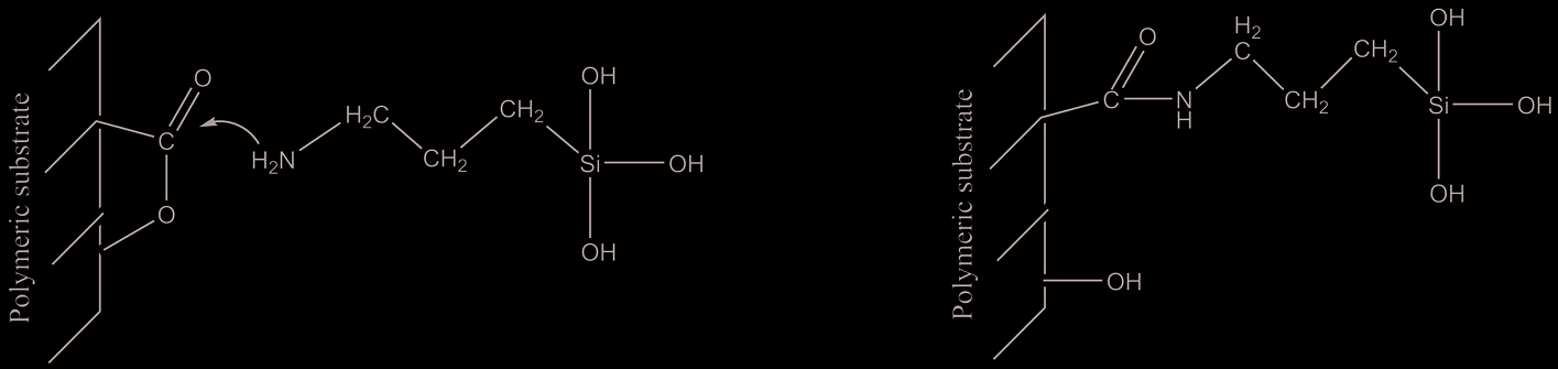
Reaction path is reported in figure 1.
The reaction proceeds through a nucleophilic attack of NH2 nitrogen atom to the carbon
atom of carbonilic group generating an amide group.
Fig. 1. Scheme of nucleophilic addition of NH2 group to the polyester carbonilic group
3.2.2 Electron Cyclotron Resonance (ECR) deposition
The deposition process was performed by ENEA Portici research centre (Naples) using
Multichamber System MC5000, a Ultra High Vacuum Multichamber for Plasma Enhanced
Chemical Vapour Deposition.
Thousand nm thick SiO2 layer was deposited by Electron Cyclotron Resonance (ECR) on a
single face of AryLiteTM substrate. During deposition process gas flows are kept constant at
2 sccm (standard cubic centimeters per minute) for SiH4, 70 sccm for H2 and 40 sccm for
N2O.
Deposition was performed for 13 minutes setting magnetron power to 400 W. Samples were
heated at 50°C under hydrogen flow for 5 minutes before SiO2 deposition. Films were
purged under nitrogen flow for 5 minutes at the end of the treatment.
3.3 Spectroscopic analysis FTIR-ATR
Infrared spectroscopic analysis has been performed by Nicolet Nexus 670 FTIR equipped
with attenuated total reflection (ATR) smart ARK HATR accessory.
In ATR, the sample is placed in optical contact on a zinc selenide (ZnSe) crystal. The IR
beam penetrate a short distance into the sample. This penetration is termed the evanescent
wave. The sample interacts with the evanescent wave, resulting in the absorption of
radiation by the sample, which closely resembles the transmission spectrum for the same
sample. However, the ATR spectrum will depend upon several parameters, including the
angle of incidence (θ) for the incoming radiation, the wavelength of the radiation (λ), and
the refractive indices of the sample (n2) and the ATR crystal (n1). The penetration depth (dp)
of the evanescent wave, is defined by equation 1.
A Study of Adhesion of Silicon Dioxide on Polymeric Substrates for Optoelectronic Applications
27
λ
dp =
(1)
2
2
2 1 /2
2π ( n 1 sen θ − n 2 )
In the 400 – 4800cm-1 wavenumber investigated range, dp varies from 5 μm to 15 μm for
measured substrates (Zuwei et al., 2007).
A spectroscopic investigation has been performed, also, by using a transmitted infrared
analysis to verify the kind of chemical reaction that occurs between polymer substrate and
organosilane.
The sample for FTIR analysis has been prepared by adding the amminosilane in a
polyarilate solution in dichloromethane solvent. In this way After treatment, films have
been obtained by solvent casting technique. They have been heated at 100 °C for 1 h in order
to remove the whole solvent. Treated films finely divided, were ground and dispersed in a
matrix of KBr (300 mg), followed by compression at 700 MPa to consolidate the formation of
the pellet for FTIR measurements.
All spectra were recorded in the range of 4000–800 cm-1.
3.4 Contact angle measurements
Contact angle measurements have been used to verify chemical surface modification. The
surface wettability was evaluated by contact angle measurements using the sessile drop
method (Mack, 1936) considering the shape of the small liquid drop to be a truncated
sphere. Prior to contact angle measurement, samples were washed in ethanol and deionised
water.
Contact angles were obtained using a Dataphysics OCA-20 contact angle analyzer with 1 μL
of liquid. A digital drop image has been processed by an image analysis system, which
calculated both the left and right contact angles from the shape of the drop with an accuracy
of ±0.1°. Drop contact angle were used to assess efficiency of surface modification suffered
by the polymer films. Each solid sample was measured ten times with liquid at room
temperature. The contact angle data were obtained at room temperature using two different
liquids: water and ethylene glycol (Ozcan & Hasirci, 2008). The contact angle is a method for
evaluation of the solid surface free energy (SFE) (van Oss et al., 1988).
3.5 Evaluation of surface free energy (SFE)
The values of SFE were obtained at room temperature using two liquids (Cantin et al., 2006)
with known surface tension (table 1). Two liquids with different polarity (P) have been
selected: water and ethylene glycol. The liquids, supplied by Aldrich, were used without
further purification.
Surface free energy of the polymer substrates was calculated using the methods proposed
by Owens and Wendt (1969) which divide the total surface free energy (γ) in 2 parts:
dispersive (γsd) and polar (γsp). The dispersive component accounts for all the London forces
such as dispersion (London–van der Waals), orientation (Keesom–van der Waals), induction
(Debye–van der Waals) and Lifshitz–van der Waals (LW) forces. The polar component is
affected by hydrogen bonding components.
The theory of contact angle of pure liquids on a solid was developed nearly 200 years ago in
terms of the Young equation (1805):
γ L cosθ = γ S + γ SL (2)
28
Optoelectronic Devices and Properties
Surface tension [mJ/m2] and Polarity
γ
γLd
γLp P
Distilled Water
72.8
21.8
51
0.70
Ethylene Glycol
48
29
19
0.40
Table 1. Surface tension data of test liquids (Ozcan & Hasirci, 2008)
where γL is the experimentally determined surface tension of the liquid, θ is the contact
angle, γS is the surface free energy of the solid and γSL is the solid–liquid interfacial energy.
In order to obtain the solid surface free energy γS an estimate of γSL has to be done. Fowkes
(1962) pioneered a surface free energy component approach. He divided the total surface
free energy in 2 parts: dispersive part and non-dispersive (or polar) part. Owens and Wendt
(1969) extended the Fowkes equation and included the hydrogen bonding term. They used
geometric mean to combine the dispersion force and hydrogen bonding components:
d d
p p
γ SL = γ S + γ L − 2 γ Sγ L − 2 γ γ
S L (3)
Dispersion force and polar components are indicated respectively by superscript d and p.
From the Young equation it follows that:
d d
p p
γ L(1 + cosθ) = 2 γ Sγ L + 2 γ γ
S L (4)
In order to obtain γSd and γSp of a solid, contact angle data for a minimum of two known
liquids are required. If two liquids are used, then, one must be polar and the other is non-
polar.
3.6 Topography measurements
Topography measurements were performed in this studies in order to investigate the
roughness of polyester films before and after surface treatment. The apparatus used in this
work was NanoTestTM Platform by Micro Materials Ltd. This instrument monitors and
records the load and displacement of a diamond three-sided pyramidal indenter tip with a
radius of curvature of about 100 nm. A constant load of 10 μN has been applied. Scans (200
μm) were collected with the tip in close proximity to the surface, but not in contact.
Nanoindenter is able to achieve sub-nanometric depth resolution in the horizontal plane.
This resolution allows for the detection of changes to topography and providing valuable
information on contribution of surface roughness to adhesion strength.
Two specimens of each film were randomly selected for recordings 20 measurements per
sample. Average surface root means squared roughness (RRMS) was calculated from
equation 5 (Faibish et al., 2002).
L
∫ ( x
2
− )
0
n
x dy
RRMS =
(5)
L
Where xn is the height of a random location on the scanned profile, x is the mean height of
all measured heights and L is the sampling scan length.
A Study of Adhesion of Silicon Dioxide on Polymeric Substrates for Optoelectronic Applications
29
3.7 Nano-indentation
Nano-indentation and nano-scratch techniques have been used in order to investigate the
adhesion between organic substrate and inorganic layer.
Hardness and elastic modulus are calculated from the load vs. displacement data obtained
by nano-indentation on coating at twenty different indentation depths ranging from 20m to
300 nm. NanoTestTM Platform, already described in section 3.6, monitors and records the
dynamic load of a three-sided pyramidal diamond indenter. Berkovich tip with a radius of
about 100 nm has been used.
In a indentation test, a Berkovich diamond tip is driven to indent the surface of the coating
from the SiO2 side. Tests were carried out in depth controlled mode, selecting a minimum
and a maximum depth of 20 nm and 300 nm respectively. The experiments were performed
with an initial load of 10 μN at loading and unloading rate of 10 µN/sec. The hold time of 30
sec at peak load was kept constant. Additional hold at 90% unload in all tests was set for
thermal drift correction.
The indenter needs to be held at the constant indentation load for a certain amount of time
in order to eliminate the dynamic effect and reach the quasi-steady flow state.
Each successive indent was displaced by 50 μm in order to avoid overlapping of plastic
deformation zone onto neighbouring indents.
All data were corrected for thermal drift and instrument compliance and subsequently
analysed with the Oliver and Pharr method (1992).
During the course of the instrumented indentation process, a record of the depth of
penetration is made, and then the area of the indent is determined using the known
geometry of the indentation tip. Indenting parameters, such as load and depth of
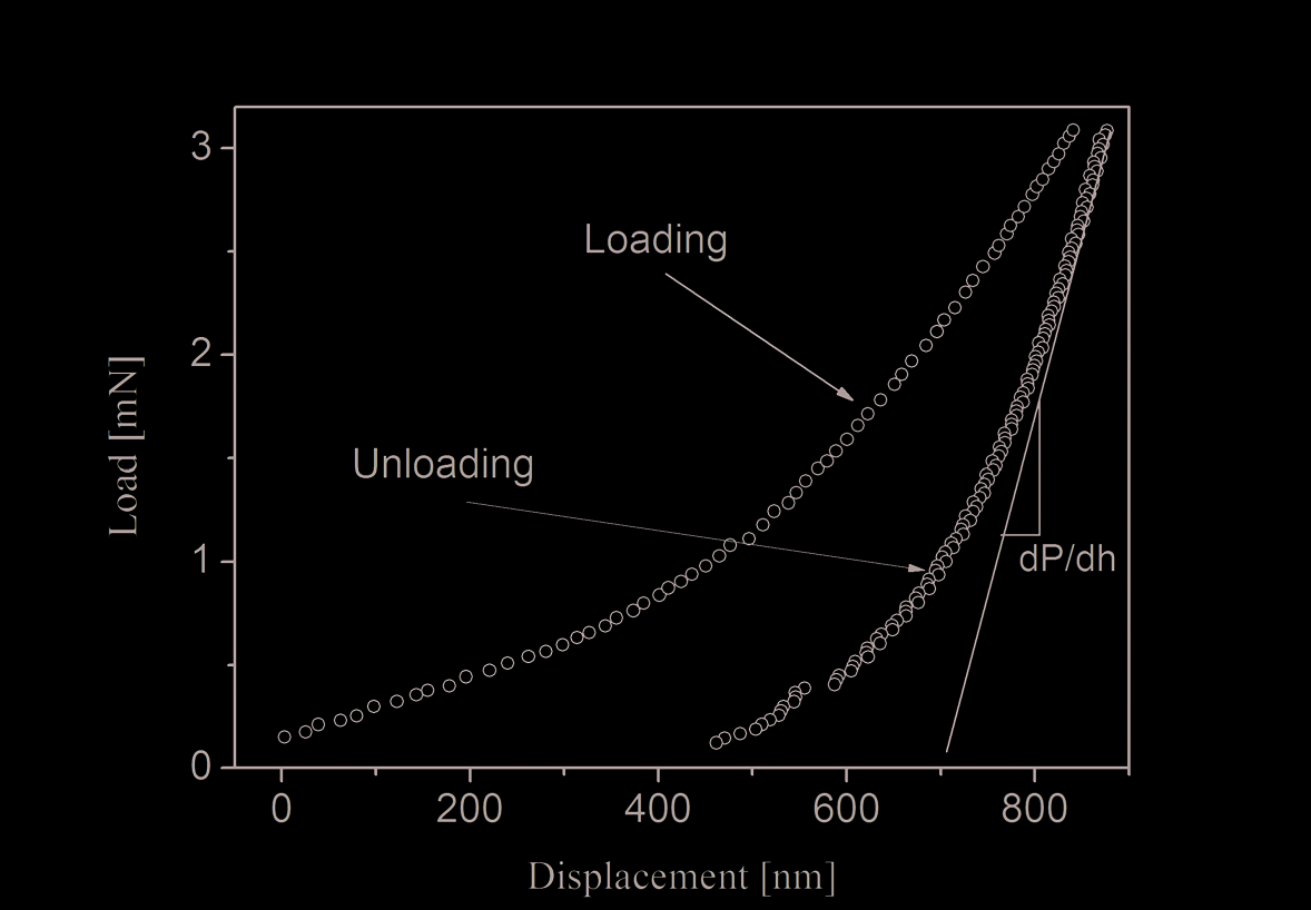
penetration, can be measured. A record of these values can be plotted on a graph to create a
load-displacement curve.
Figure 2 shows a typical loading and unloading displacement curves during a
nanoindentation cycle on AryLiteTM. A power law curve was fit to the unload data points.
Fig. 2. Typical loading and unloading displacement curves during a nanoindentation cycle
on AryLiteTM substrate
30
Optoelectronic Devices and Properties
The slope dP/dh at the maximum load data point is used to calculate the elastic modulus
(Er). Hardness is calculated by dividing the loading force by the projected residual area of
the indentation. Hardness and the Young’s modulus of elasticity can be obtained from the
slope of the unloading curve. The hysteresis indicates that the deformation is not fully
elastic and partially inelastic.
3.8 Nano-Scratch test
In nano-scratch studies a conical indenter is drawn over the sample surface with ramping
up of the load until damage occurs. The load corresponding to this damage provides a
measure of scratch resistance or adhesive strength of a coating and is called the “critical
load” (Park & Kwon, 1997). The definition of damage can be the onset of cracking around
the scratching tip, spalling of the coating, or the formation of a channel in which all of the
coating has been removed from the substrate. The critical loads are indicators of the scratch
resistance of these samples.
Scratches have been made by translating the sample while ramping the loads on the conical
diamond tip (1μm tip radius) over different load ranges from 0 mN to 10 mN. A sudden
increase in the scratch load was related to coating damage.
Multipass test experiments have been performed. They consist of three sequential scans over
the same 250 µm track, all at 2 µm/sec scan speed. In the first topography scan the applied
load was constant at 100 μN. Surface roughness was measured from this scan. In the second
scratch scan, the load applied after 50 µm was ramped at a constant rate of 0.1 mN/sec to a
maximum load reached of 10 mN. In the final scan the resultant topography was observed
by using a low applied load of 100 μN. Five repeat tests were performed on each sample.
4. Results and discussion
4.1 Thermo-Mechanical properties of AryLiteTM
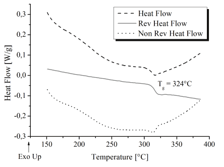
AryLiteTM exhibits excellent Tg (324°C) (figure 3) and good optical transparency. The lack of
crystalline phase is a consequence of the aromatic and rigid nature of the polymer backbone
which hinders conformational rearrangements into a regular crystalline structure. On the
other hand the rigid backbone is responsible of reduced elongation at break and the lack of
crystalline reinforcement results in poor elastic and ultimate properties (table 2).
The initial degradation temperatures (Tid) have been measured by using thermogravimetric
analyser at a scanning rate of 10°C/min in N2 purging flow. Tid is associated to 3 % weight
loss.
Thermal and mechanical behavior of polyester indicate that AryLiteTM is a good candidate
for optoelectronic application.
Thermal and mechanical properties of AryLiteTM are shown in table 2.
AryLiteTM
Glass transition temperature Tg [°C]
324
Initial degradation temperature [°C]
488
Young’s Modulus Es [GPa]
2.82±0.24
Elongation at break εr [%] 10.24±2.56
Table 2. Thermo-mechanical properties of AryliteTM
A Study of Adhesion of Silicon Dioxide on Polymeric Substrates for Optoelectronic Applications
31
Fig. 3. Modulated Differential Scanning Calorimetry of AryLiteTM.
4.2 Spectroscopic analysis FTIR-ATR
Infrared spectroscopic analysis has been performed to verify the reaction between amino
group located on the organo-silane and carboxylic group of polymeric substrate.
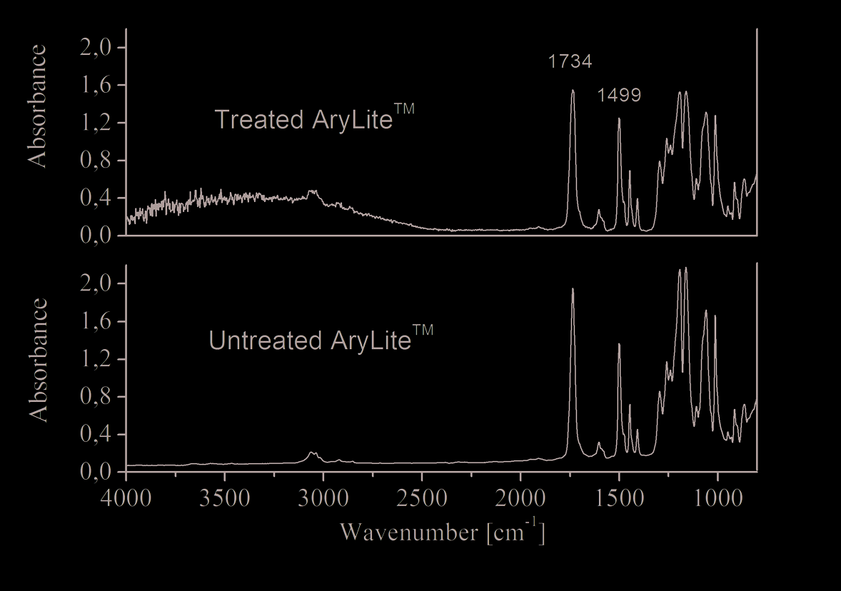
In figure 4 normalized ATR spectra of untreated AryLiteTM and AryLiteTM treated with
APTEOS solution have been plotted.
Fig. 4. ATR spectra of AryLiteTM before and after surface silane treatment in the range 4000-
700 cm-1
32
Optoelectronic Devices and Properties
In order to make a comparison between the treated and untreated samples the intensity of
each peak was rationed (Gu et al., 2001) against the absorbance of the invariant band at 1499
cm-1. These peaks are due to C-H in-plane bending of the benzene ring.
In the FTIR-ATR spectra, silane-treated specimens show a wide peak between about 2500 –
4000 cm-1. This is attributable to the presence of SiOH groups (Anderson & Smith, 1974).
Treated sample spectra show a decrease of C=O ester linkage at 1734 cm-1 and a decrease of
C–O ester stretching vibrations in the region 1300 – 1000 cm-1 after silane treatment
(Bellamy, 1975) (Colthup et al., 1990).
This is attributable to nucleophilic addition of the amine group (NH2) to the carbonilic
group. Following this reaction path, the organosilane APTEOS has been grafted on the
AryLiteTM substrate.
In fact, a chemical reaction could happen between amine group (NH2) of silane and
carbonilic group of polymer substrate. The reaction produce an amide group (O=C-NH).
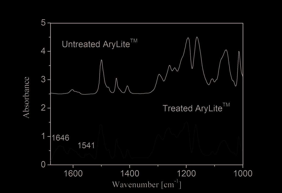
This hypothesis has been supported by a spectroscopic study. Figure 5 shows double peak
of amide group located at about 1640-1540 cm-1.
Fig. 5. FTIR spectra of polyarilate before and after silane treatment in a dichloromethane
solution
4.3 Contact angle measurements
AryLiteTM is an hydrophobic film with a water contact angle of 92 degrees. Samples treated
with silane show a decrease of water contact angle of about 20 degrees. It has been
demonstrated that silane treatment is effective in increasing the hydrophilicity of samples.
4.4 Evaluation of surface free energy (SFE)
In order to obtain γSd and γSp of a solid, contact angle data for a minimum of two known
liquids are required. If two liquids are used, then, one must be polar and other is non-polar.
In this study two test liquids were used as a probe for surface free energy calculations:
distilled water and ethylene glycol. The data for surface tension components of the test
liquids at 20 °C are given in table 1.
A Study of Adhesion of Silicon Dioxide on Polymeric Substrates for Optoelectronic Applications
33
Silane treatment binds OH groups on the polymeric surface. This phenomenon increase
polyester surface polarity and surface free energy (Clint, 2001) (table 3). The increase in
surface polarity causes an increase in molecular forces between substrates and hence an
increase in adhesion strength (Burnett et al., 2007) (Comyn, 1992) (Lee & Wool, 2002).
In table 3 are reported SFE of untreated AryLiteTM and treated AryLiteTM calculated by
using geometric mean method (Spelt et al., 1996).
Surface Free Energy [mJ/m2]
γ
γSd
γSp P
Untreated AryLiteTM
29.97 27.80 2.17 0.07
Treated AryLiteTM
30.19 17.10 13.09 0.43
Table 3. Surface free energy and polarity of AryLiteTM films before and after surface
treatment
4.5 Topography measurements
The topography scan technique was used to measure the roughness of samples before and
after the silane treatments.
The changes of surface roughness produce a surface topography variation and provide a
contribution to substrates adhesion strength.
Untreated AryLiteTM films are smooth and they possess the lower roughness value of about
2.64±0.57 nm. Treated and untreated samples exhibit a root means squared roughness (RRMS)
lower than 20 nm. All materials can be considered as totally flat from a topographic point of
view (Ponsonnet et al., 2003).
Clearly, surface roughness of the treated polymers was higher than the untreated polyester.
After the chemical treatment AryLiteTM, exhibit a RRMS value 2.7 times higher than