ECE 320 Spring 2004 by Mark Butala, et al - HTML preview
Download the book in PDF, ePub for a complete version.
auxiliary registers (ARx) to manage pointers with integer increments. The auxiliary registers are
not suited for the non-integer pointers needed in this exercise, however, so another method is
required. One possibility is to perform addition in the accumulator with a modified decimal point.
For example, with N=256 , you need eight bits to represent the integer portion of your pointer.
Interpret the low 16 bits of the accumulator to have a decimal point seven bits up from the
bottom; this leaves nine bits to store the integer part above the decimal point. To increment the
pointer by one step, add a 15-bit value to the low part of the accumulator, then zero the top bit to
ensure that the value in the accumulator is greater than or equal to zero and less than 256.[9] To


use the integer part of this pointer, shift the accumulator contents seven bits to the right, add the
starting address of the sine table, and store the low part into an ARx register. The auxiliary
register now points to the correct sample in the sine table.
As an example, for a nominal carrier frequency
and sine table length N=256 , the nominal
step size is an integer
. Interpret the 16-bit pointer as having nine bits for the integer
part, followed by a decimal point and seven bits for the fractional part. The corresponding literal
(integer) value added to the accumulator would be 16×27=2048 .[10]
Extensions
You may want to refer to Proakis [link] and Blahut [link]. These references may help you think about the following questions:
How does the noise affect the described carrier recovery method?
What should the phase-detector look like for a BPSK modulated carrier? (Hint: You would need
to consider both the in-phase and quadrature channels.)
How does α affect the bandwidth of the loop filter?
How do the loop gain and the bandwidth of the loop filter affect the PLL's ability to lock on to a
carrier frequency mismatch?
References
1. J.G. Proakis. (1995). Digital Communications. (3rd edition). McGraw-Hill.
2. R. Blahut. (1990). Digital Transmission of Information. Addison-Wesley.
Digital Receivers: Symbol-Timing Recovery for QPSK*
Introduction
This receiver exercise introduces the primary components of a QPSK receiver with specific focus
on symbol-timing recovery. In a receiver, the received signal is first coherently demodulated and
low-pass filtered (see Digital Receivers: Carrier Recovery for QPSK) to recover the message signals (in-phase and quadrature channels). The next step for the receiver is to sample the message
signals at the symbol rate and decide which symbols were sent. Although the symbol rate is
typically known to the receiver, the receiver does not know when to sample the signal for the best
noise performance. The objective of the symbol-timing recovery loop is to find the best time to


sample the received signal.
Figure 2.8 illustrates the digital receiver system. The transmitted signal coherently demodulated with both a sine and cosine, then low-pass filtered to remove the double-frequency terms, yielding
the recovered in-phase and quadrature signals,
and
. These operations are explained in
Digital Receivers: Carrier Recovery for QPSK. The remaining operations are explained in this module. Both branches are fed through a matched filter and re-sampled at the symbol rate. The
matched filter is simply an FIR filter with an impulse response matched to the transmitted pulse.
It aids in timing recovery and helps suppress the effects of noise.
Figure 2.8.
Digital receiver system
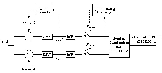
If we consider the square wave shown in Figure 2.9 as a potential recovered in-phase (or
quadrature) signal ( i.e. , we sent the data [+1, -1, +1, -1, …] ) then sampling at any point other
than the symbol transitions will result in the correct data.
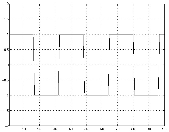
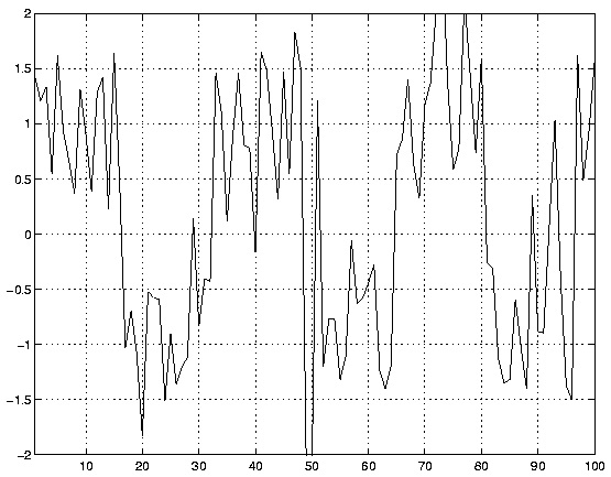
Figure 2.9.
Clean BPSK waveform.
Figure 2.10.
Noisy BPSK waveform.
However, in the presence of noise, the received waveform may look like that shown in
Figure 2.10. In this case, sampling at any point other than the symbol transitions does not
guarantee a correct data decision. By averaging over the symbol duration we can obtain a better
estimate of the true data bit being sent ( +1 or -1 ). The best averaging filter is the matched filter,
which has the impulse response u[ n]− u[ n− T symb] , where u[ n] is the unit step function, for the
simple rectangular pulse shape used in Digital Transmitter: Introduction to Quadrature Phase-
Shift Keying. [11]Figure 2.11 and Figure 2.12 show the result of passing both the clean and noisy
signal through the matched filter.
Figure 2.11.
Averaging filter output for clean input.
Figure 2.12.
Averaging filter output for noisy input.
Note that in both cases the output of the matched filter has peaks where the matched filter exactly
lines up with the symbol, and a positive peak indicates a +1 was sent; likewise, a negative peak
indicates a -1 was sent. Although there is still some noise in second figure, the peaks are relatively
easy to distinguish and yield considerably more accurate estimation of the data ( +1 or -1 ) than
we could get by sampling the original noisy signal in Figure 2.10.
The remainder of this handout describes a symbol-timing recovery loop for a BPSK signal
(equivalent to a QPSK signal where only the in-phase signal is used). As with the above examples,
a symbol period of Ts=16 samples is assumed.
Early/late sampling
One simple method for recovering symbol timing is performed using a delay-locked loop ( DLL).
Figure 2.13 is a block diagram of the necessary components.
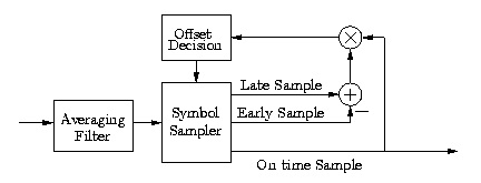
Figure 2.13.
DLL block diagram.
Consider the sawtooth waveform shown in Figure 2.11, the output of the matched filter with a
square wave as input. The goal of the DLL is to sample this waveform at the peaks in order to
obtain the best performance in the presence of noise. If it is not sampling at the peaks, we say it is
sampling too early or too late.
The DLL will find peaks without assistance from the user. When it begins running, it arbitrarily
selects a sample, called the on-time sample, from the matched filter output. The sample from the
time-index one greater than that of the on-time sample is the late sample, and the sample from
the time-index one less than that of the on-time sample is the early sample. Figure 2.14 shows an example of the on-time, late, and early samples. Note in this case that the on-time sample happens
to be at a peak in the waveform. Figure 2.15 and Figure 2.16 show examples in which the on-time sample comes before a peak and after the peak.
The on-time sample is the output of the DLL and will be used to decide the data bit sent. To
achieve the best performance in the presence of noise, the DLL must adjust the timing of on-time
samples to coincide with peaks in the waveform. It does this by changing the number of time-
indices between on-time samples. There are three cases:
1. In Figure 2.14, the on-time sample is already at the peak, and the receiver knows that peaks are spaced by T symb samples. If it then takes the next on-time sample T symb samples after this on-time sample, it will be at another peak.
2. In Figure 2.15, the on-time sample is too early. Taking an on-time sample T symb samples later will be too early for the next peak. To move closer to the next peak, the next on-time sample is
taken T symb+1 samples after the current on-time sample.
3. In Figure 2.16, the on-time sample is too late. Taking an on-time sample T symb samples later will be too late for the next peak. To move closer to the next peak, the next on-time sample is
taken T symb−1 samples after the current on-time sample.
The offset decision block uses the on-time, early, and late samples to determine whether sampling
is at a peak, too early, or too late. It then sets the time at which the next on-time sample is taken.
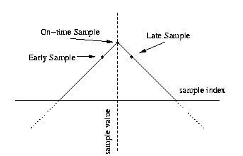
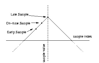
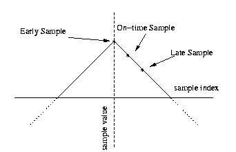
Figure 2.14.
Sampling at a peak.
Figure 2.15.
Sampling too early.
Figure 2.16.
Sampling too late.
The input to the offset decision block is on-time(late−early) , called the decision statistic.
Convince yourself that when the decision statistic is positive, the on-time sample is too early,
when it is zero, the on-time sample is at a peak, and when it is negative, the on-time sample is too
late. It may help to refer to Figure 2.14, Figure 2.15, and Figure 2.16. Can you see why it is necessary to multiply by the on-time sample?
The offset decision block could adjust the time at which the next on-time sample is taken based
only on the decision statistic. However, in the presence of noise, the decision statistic becomes a
less reliable indicator. For that reason, the DLL adds many successive decision statistics and
corrects timing only if the sum exceeds a threshold; otherwise, the next on-time sample is taken
T symb samples after the current on-time sample. The assumption is that errors in the decision
statistic caused by noise, some positive and some negative, will tend to cancel each other out in
the sum, and the sum will not exceed the threshold because of noise alone. On the other hand, if
the on-time sample is consistently too early or too late, the magnitude of the added decision
statistics will continue to grow and exceed the threshold. When that happens, the offset decision
block will correct the timing and reset the sum to zero.
Sampling counter
The symbol sampler maintains a counter that decrements every time a new sample arrives at the
output of the matched filter. When the counter reaches three, the matched-filter output is saved as
the late sample, when the counter reaches two, the matched-filter output is saved as the on-time
sample, and when the counter reaches one, the matched-filter output is saved as the early sample.
After saving the early sample, the counter is reset to either T symb−1 , T symb , or T symb+1 ,
according to the offset decision block.
MATLAB Simulation
Because the DLL requires a feedback loop, you will have to simulate it on a sample-by-sample
basis in MATLAB.
Using a square wave of period 32 samples as input, simulate the DLL system shown in
Figure 2.13. Your input should be several hundred periods long. What does it model? Set the
decision-statistic sum-threshold to 1.0 ; later, you can experiment with different values. How do
you expect different thresholds to affect the DLL?
Figure 2.17 and Figure 2.18 show the matched filter output and the on-time sampling times (indicated by the impulses) for the beginning of the input, before the DLL has locked on, as well
as after 1000 samples (about 63 symbols' worth), when symbol-timing lock has been achieved. For
each case, note the distance between the on-time sampling times and the peaks of the matched
filter output.
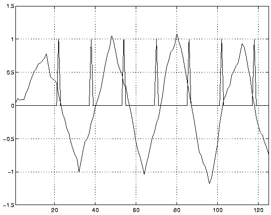
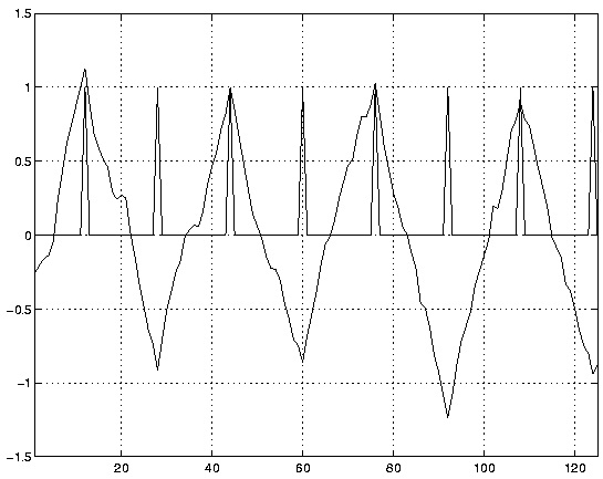
Figure 2.17.
Symbol sampling before DLL lock.
Figure 2.18.
Symbol sampling after DLL lock.
DSP Implementation
Once your MATLAB simulation works, DSP implementation is relatively straightforward. To test
your implementation, you can use the function generator to simulate a BPSK waveform by setting
it to a square wave of the correct frequency for your symbol period. You should send the on-time
sample and the matched-filter output to the D/A to verify that your system is working.
Extensions
As your final project will require some modification to the discussed BPSK signaling, you will
want to refer to the listed references, (see Proakis [link] and Blahut [link], and consider some of the following questions regarding such modifications:
How much noise is necessary to disrupt the DLL?
What happens when the symbol sequence is random (not simply [+1, -1, +1, -1, …] )?
What would the matched filter look like for different symbol shapes?
What other methods of symbol-timing recovery are available for your application?
How does adding decision statistics help suppress the effects of noise?
References
1. J.G. Proakis. (1995). Digital Communications. (3rd edition). McGraw-Hill.
2. R. Blahut. (1990). Digital Transmission of Information. Addison-Wesley.
2.4. Video Processing
Video Processing Manuals*
Essential documentation for the 6000 series TI DSP
The following documentation will certainly prove useful:
The IDK User's Guide
The IDK User's Guide
The IDK Video Device Drivers User's Guide
Note
Other manuals may be found on TI's website by searching for TMS320C6000 IDK
Video Processing Part 1: Introductory Exercise*
Introduction
The purpose of this lab is to acquaint you with the TI Image Developers Kit (IDK). The IDK
contains a floating point C6711 DSP, and other hardware that enables real time video/image
processing. In addition to the IDK, the video processing lab bench is equipped with an NTSC
camera and a standard color computer monitor.
You will complete an introductory exercise to gain familiarity with the IDK programming
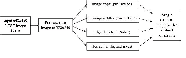
environment. In the exercise, you will modify a C skeleton to horizontally flip and invert video
input (black and white) from the camera. The output of your video processing algorithm will
appear in the top right quadrant of the monitor.
In addition, you will analyze existing C code that implements filtering and edge detection
algorithms to gain insight into IDK programming methods. The output of these "canned"
algorithms, along with the unprocessed input, appears in the other quadrants of the monitor.
Finally, you will create an auto contrast function. And will also work with a color video feed and
create a basic user interface, which uses the input to control some aspect of the display.
An additional goal of this lab is to give you the opportunity to discover tools for developing an
original project using the IDK.
Important Documentation
The following documentation will certainly prove useful:
The IDK User's Guide. Section 2 is the most important.
The IDK Video Device Drivers User's Guide. The sections on timing are not too important, but pay attention to the Display and Capture systems and have a good idea of how they work.
The IDK Programmer's Guide. Sections 2 and 5 are the ones needed. Section 2 is very, very important in Project Lab 2. It is also useful in understanding “streams” in project lab 1.
Note
Other manuals may be found on TI's website by searching for TMS320C6000 IDK
Video Processing - The Basics
The camera on the video processing lab bench generates a video signal in NTSC format. NTSC is
a standard for transmitting and displaying video that is used in television. The signal from the
camera is connected to the "composite input" on the IDK board (the yellow plug). This is
illustrated in Figure 2-1 on page 2-3 of the IDK User's Guide. Notice that the IDK board is
actually two boards stacked on top of each other. The bottom board contains the C6711 DSP,
where your image processing algorithms will run. The daughterboard is on top, it contains the
hardware for interfacing with the camera input and monitor output. For future video processing
projects, you may connect a video input other than the camera, such as the output from a DVD
player. The output signal from the IDK is in RGB format, so that it may be displayed on a
computer monitor.
At this point, a description of the essential terminology of the IDK environment is in order. The
video input is first decoded and then sent to the FPGA, which resides on the daughterboard. The
FPGA is responsible for video capture and for the filling of the input frame buffer (whose contents
we will read). For a detailed description of the FPGA and its functionality, we advise you to read
Chapter 2 of the IDK User's Guide.
The Chip Support Library (CSL) is an abstraction layer that allows the IDK daughterboard to be
used with the entire family of TI C6000 DSPs (not just the C6711 that we're using); it takes care
of what is different from chip to chip.
The Image Data Manager (IDM) is a set of routines responsible for moving data between on-chip
internal memory, and external memory on the board, during processing. The IDM helps the
programmer by taking care of the pointer updates and buffer management involved in transferring
data. Your DSP algorithms will read and write to internal memory, and the IDM will transfer this
data to and from external memory. Examples of external memory include temporary "scratch pad"
buffers, the input buffer containing data from the camera, and the output buffer with data destined
for the RGB output.
The two different memory units exist to provide rapid access to a larger memory capacity. The
external memory is very large in size – around 16 MB, but is slow to access. But the internal is
only about 25 KB or so and offers very fast access times. Thus we often store large pieces of data,
such as the entire input frame, in the external memory. We then bring it in to internal memory,
one small portion at a time, as needed. A portion could be a line or part of a line of the frame. We
then process the data in internal memory and then repeat in reverse, by outputting the results line
by line (or part of) to external memory. This is full explained in Project Lab 2, and this
manipulation of memory is important in designing efficient systems.
The TI C6711 DSP uses a different instruction set than the 5400 DSP's you are familiar with in
lab. The IDK environment was designed with high level programming in mind, so that
programmers would be isolated from the intricacies of assembly programming. Therefore, we
strongly suggest that you do all your programming in C. Programs on the IDK typically consist of
a main program that calls an image processing routine.
The main program serves to setup the memory spaces needed and store the pointers to these in
objects for easy access. It also sets up the input and output channels and the hardware modes
(color/grayscale ...). In short it prepares the system for our image processing algorithm.
The image processing routine may make several calls to specialized functions. These specialized
functions consist of an outer wrapper and an inner component. The wrapper oversees the
processing of the entire image, while the component function works on parts of an image at a
time. And the IDM moves data back and forth between internal and external memory.
As it brings in one line in from external memory, the component function performs the processing
on this one line. Results are sent back to the wrapper. And finally the wrapper contains the IDM
instructions to pass the output to external memory or wherever else it may be needed.
Please note that this is a good methodology used in programming for the IDK. However it is very
flexible too, the "wrapper" and "component functions" are C functions and return values, take in
parameters and so on too. And it is possible to extract/output multiple lines or block etc. as later
shown.
In this lab, you will modify a component to implement the flipping and inverting algorithm. And
you will perform some simple auto-contrasting as well as work with color.
In addition, the version of Code Composer that the IDK uses is different from the one you have
used previously. The IDK uses Code Composer Studio v2.1. It is similar to the other version, but
the process of loading code is slightly different.
Code Description
Overview and I/O
The next few sections describe the code used. First please copy the files needed by following the
instructions in the "Part 1" section of this document. This will help you easily follow the next few
parts.
The program flow for image processing applications may be a bit different from your previous
experiences in C programming. In most C programs, the main function is where program
execution starts and ends. In this real-time application, the main function serves only to setup
initializations for the cache, the CSL, and the DMA (memory access) channel. When it exits, the
main task, tskMainFunc(), will execute automatically, starting the DSP/BIOS. It will loop
continuously calling functions to operate on new frames and this is where our image processing
application begins.
The tskMainFunc(), in main.c, opens the handles to the board for image capture (VCAP_open())
and to the display (VCAP_open()) and calls the grayscale function. Here, several data structures
are instantiated that are defined in the file img_proc.h. The IMAGE structures will point to the
data that is captured by the FPGA and the data that will be output to the display. The
SCRATCH_PAD structure points to our internal and external memory buffers used for temporary
storage during processing. LPF_PARAMS is used to store filter coefficients for the low pass filter.
The call to img_proc() takes us to the file img_proc.c. First, several variables are declared and
defined. The variable quadrant will denote on which quadrant of the screen we currently want
output; out_ptr will point to the current output spot in the output image; and pitch refers to the
byte offset (distance) between two lines. This function is the high level control for our image-
processing algorithm. See algorithm flow.