Nanotechnology: Content and Context by Christopher Kelty, John S. Hutchinson - HTML preview
Download the book in PDF, ePub for a complete version.
Chapter 2. Some Basic Science for Nano
2.1. Beyond Optical Microscopy*
"This module was developed as part of a Rice University Class called "Nanotechnology: Content and Context" initially funded by the National Science Foundation under Grant No. EEC-0407237. It was conceived, researched, written and edited by students in the Fall 2005 version of the class, and reviewed by participating professors."
Introduction
Light microscopes are used in a number of areas such as medicine, science, and engineering. However, light microscopes cannot give us the high magnifications needed to see the tiniest objects like atoms. As the study of both microstructures and macrostructures of materials have come to the forefront of materials research and development new methods and equipment have been developed. Both the usage of electrons and atomic force rather than light permits advanced degrees of observations than would allow an optical microscope. As the interest in new materials in general and nanomaterials in particular is growing alternatives to optical microscopy are proving fundamental to the advancement of nanoscale science and technology.
Scanning Electron Microscope
SEM: A Brief History
The scanning electron microscope is an incredible tool for seeing the unseen worlds of microspace. The scanning electron microscope reveals new levels of detail and complexity in the world of micro-organisms and miniature structures. While conventional light microscopes use a series of glass lenses to bend light waves and create a magnified image, the scanning electron microscope creates magnified images by using electrons instead of light waves.
The earliest known work describing the conceptualization of the scanning electron microscope was in 1935 by M. Knoll who, along with other pioneers in the field of electron optics, was working in Germany. Although it was Manfred von Ardenne who laid the foundations of both transmission and surface scanning electron microscopy just before World War II, it is Charles Oatley who is recognized as the great innovator of scanning electron microscopy. Oatley’s involvement with the SEM began immediately after World War II when, his recent wartime experience in the development of radar, allowed him to develop new techniques that could be brought to overcome some of the fundamental problems encountered by von Ardenne in his pre-war research.
Von Ardenne (1938) constructed a scanning transmission electron microscope (STEM) by adding scan coils to a transmission electron microscope. [1] In the late 1940s Oatley, then a lecturer in the Engineering Department of Cambridge University, England, showed interest in conducting research in the field of electron optics and decided to re-investigate the SEM as an accompaniment to the work being done on the TEM (by V. E. Cosslett, also being developed in Cambridge at the Physics Department). One of Oatley's students, Ken Sander, began working on a column for a transmission electron microscope using electrostatic lenses, but after a long period of illness was forced to suspend his research. His work then was taken up by Dennis McMullan in 1948, when he and Oatley built their first SEM by 1951. By 1952 this instrument had achieved a resolution of 50 nm.
How the SEM works
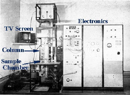
In the SEM, electromagnets are used to bend an electron beam which is then utilized to produce the image on a screen. The beam of electrons is produced at the top of the microscope by heating a metallic filament. The electron beam follows a vertical path through the column of the microscope. It makes its way through electromagnetic lenses which focus and direct the beam down towards the sample. Once it hits the sample, other electrons are ejected from the sample. Detectors collect the secondary or backscattered electrons, and convert them to a signal that is sent to a viewing screen similar to the one in an ordinary television, producing an image.
By using electromagnets an observer can have more control over how much magnification he/she obtains. The SEM has a large depth of field, which allows a large amount of the sample to be in focus at one time. The electron beam also provides greater clarity in the image produced. The SEM allows a greater depth of focus than the optical microscope. For this reason the SEM can produce an image that is a good representation of the three-dimensional sample.
The SEM also produces images of high resolution, which means that closely spaced features can be examined at a high magnification. Preparation of the samples is relatively easy since most SEMs only require the sample to be conductive. The combination of higher magnification, larger depth of focus, greater resolution, and ease of sample observation makes the SEM one of the most heavily used instruments in research areas today.
SEM Usage
The SEM is designed for direct studying of:
Topography: study of the surfaces of solid objects
Morphology: study of shape and size
Brief history of each microscope
Composition: analysis of elements and compounds
Crystallographic information: how atoms are arranged in a sample
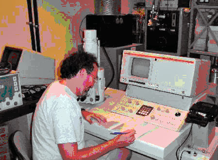
SEM has become one of the most widely utilized instruments for material characterization. Given the overwhelming importance and widespread use of the SEM, it has become a fundamental instrument in universities and colleges with materials-oriented programs. [2] Institutions of higher learning and research have been forced to take extremely precautious measures with their equipment as it is expensive and maintenance is also costly.
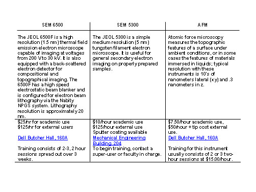
Rice University, for example, has created what is called the Rice Shared Equipment Authority (SEA) to organize schedules, conduct training sessions, collect usage fees and maintain the usage of its high tech microscopic equipment. The following chart indicates prices, location, and necessary training for three of the most popular instruments under SEA jurisdiction:
Advantages and Disadvantages
Among the advantages is the most obvious, better resolution and depth of field than light microscopes. The SEM also provides compositional information for small areas, is relatively easy to use (after training), and the coatings make it semi non-destructive to beam damage. Its disadvantages, however, are all related to the specimen being examined. There are occasions when vacuum compatibility does not allow clear visibility. Specimen preparation can also cause contamination by introducing unwanted artifacts. Lastly, specimen must also be conductive for maximum visibility.
What makes the SEM such a useful instrument? What can it do that a normal optical microscope cannot?
Explain the usage of the electron beam in the SEM.
What is meant by “images of high resolution"?
Scanning Tunneling Microscopes
A Brief Historical Note
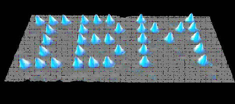
The scanning tunneling microscope (STM) had its birth in 1981, invented by Gerd Binnig and Heinrich Rohrer of IBM, in Zurich, Germany. They won the 1986 Nobel Prize in physics for this accomplishment, but use of the microscope itself was somewhat slow to spread into the academic world. STM is used to scan surfaces at the atomic level, producing a map of electron densities; the surface science community was somewhat skeptical and resistant of such a pertinent tool coming from an outside, industrial source. There were questions as to the interpretations of the early images (how are we really sure those are the individual silicon atoms?), as well as the difficulty of interpreting them in the first place – the original STMs did not include computers to integrate the data. The older electron microscopes were generally easier to use, and more reliable; hence they retained preference over STMs for several years after the STM development. STM gained publicity slowly, through accomplishments such as IBM’s famous xenon atom arrangement feat (see fig. 3) in 1990, and the determination of the structure of “crystalline” silicon.
How STMs Work: The Basic Ideas
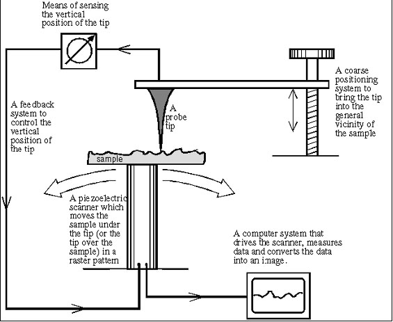
| I. The Probe: Scanning Tunneling Microscopy relies on a tiny probe of tungsten, platinum-iridium, or another conductive material to collect the data. The probe slowly “scans” across a surface, yielding an electron-density map of the nanoscale features of the surface. To achieve this resolution, the probe must be a wire with a protruding peak of a single atom; the sharper the peak, the better the resolution. A voltage difference between the tip and the sample results in an electron “tunneling” current when the tip comes close enough (within around 10 Å). This “tunneling” is a phenomenon explained by the quantum mechanical properties of particles; the current is either held constant and probe height recorded, or the probe’s height is maintained and the change in current is measured to produce the scanning data. In constant current microscopy, the probe height must be constantly adjusted, which makes for relatively slow scanning, but allows fairly irregular surfaces to be examined. By contrast, constant height mode allows for faster scanning, but will only be effective for relatively smooth sample surfaces. |
| II. Piezoelectric Scanner: In order to make the sub-nanometer vertical adjustments required for STM, piezoelectric ceramics are used in the scanning platform on which the sample is held. Piezoelectric materials undergo infinitesimally small mechanical changes under an applied voltage; therefore in the positioning device of a STM, they provide the motion to change the tip height at small enough increments that collision with the sample surface can be avoided. A data feedback loop is maintained between probe and piezoelectric positioner, so that the tip’s height can be adjusted as necessary in constant-current mode, and can be brought close enough to the sample to begin scanning in the first place. |
| III. The Computer: Though the earliest STMs did not include a computer with the scanning apparatus, current models have one attached to filter and integrate the data as it is received, as well as to monitor and control the actual scanning process. Grayscale primary images can be colored to give contrast to different types of atoms in the sample; most published STM images have been enhanced in this way. |
The very high degree of focus of a STM allows it to be used as a spectroscopic tool as well as a larger scale image producer. Properties of a single point on a sample surface can be analyzed through focused examination of the electronic structure.
Complications and Caveats
The integral use of the tunneling current in STM requires that both the probe and the sample be conductive, so the electrons can move between them. Non-conductive samples, therefore, must be coated in a metal, which obscures details as well as masks the actual properties of the sample. Furthermore, like with the SEM, oxidation and other contamination of the sample surface can be a problem, depending on the material(s) being studied. To avoid this, STM work is often carried out in an ultra-high vacuum (UHV) environment rather than in air. Some samples, however, are fairly well-suited to study in ambient conditions; one can strip away successive levels of a layered sample material in order to “clean” the surface as the study is being conducted.
Another seemingly simple problem involved in STM is control of vibration. Since the distances between probe and sample are so minute, the tiniest shake can result in data errors or cause the tip to collide with the surface, damaging the sample and possibly ruining the tip of the probe. A variety of systems have been implemented to control vibration, often involving frames with springs, or a sling in which the microscope is hung.
STM is plagued by artifacts, systematic errors in the observed data due to the mechanistic details of the microscope. For example, repetition of a particular shape in the same orientation throughout the image may be a case of tip artifacts, where a feature on the sample was sharper than the tip itself, resulting in the tip’s shape being recorded rather than that of the sample feature. Lack of optimization of the microscope’s feedback loop can produce large amounts of noise in the data, or, alternatively, cause a surface to be much smoother than it is. Finally, while sophisticated image processing software lends much-needed clarity to STM data, it can be misused such that meaning is created where there is none. Image filters used must be carefully evaluated against more “raw” image data to affirm their utility.
Counterbalancing the technique’s obvious usefulness is the general difficulty of STM as a process. Whereas a scanning electron microscope can be operated successfully by a researcher with minimum skills as a technician, STMs are notoriously finicky and require expertise, time, and patience to produce a decent image. They are therefore not particularly popular research tools, though improvements in design and artifact control have been and are being made, making STM increasingly more practical.
In what types of situations would constant current microscopy be preferred over constant height? And vice-versa?
What are potential problems of the large amount of data filtering and processing involved in STM?
What errors are likely to be present in data from a particularly jagged, sharp-featured sample, and why?
Atomic Force Microscope
Another New Microscope
The requirement to have a conducting sample limited the usefulness of the STM. Gerd Binnig, Christoph Gerber, and Calvin Quate solved this problem with the invention of the Atomic Force Microscope (AFM) in 1986. [3] As suggested by its name, the AFM uses atomic forces—not the flow of electrons—to scan a sample, so it can be inductive as well as conductive. Still, the set up of the two microscopes is similar (see Figure 6). The AFM has a sharp tip a few micrometers long and usually a diameter less than 100 Å. It is attached to the end of a flexible tube 100-200 µm in length called a cantilever. The tip is brought close enough to the sample to feel forces that contribute to atomic bonds, called van der Waals forces. These are due to the attraction and repulsion of positively-charged protons and negatively-charged electrons. As electrons zip around an atom, they create temporary regions of positive and negative charges, which attract oppositely-charged regions on other atoms. If the atoms get too close, though, the repulsive force of the electrons overshadows this weaker attraction. In terms of the AFM, the temporary positive and negative charges attract the atoms in the tip and sample when they are far apart (several angstroms), but if they come too close (1-2 Å, less than the length of an atomic bond), the electrons on the tip and sample repel each other. This feature led to the development of two types of AFM: contact and non-contact.
The Contact AFM
A contact AFM is so called because the tip and the sample are closer to each other than atoms of the same molecule are. (It is difficult to define “contact” at the molecular level; bonds form when electrons from different atoms overlap. There is no rubbing together of atoms as we think of it at the macrolevel.) Since the cantilever is flexible, it is sensitive to the mutually repulsive force exerted between the tip and sample. This force varies with the topography of the latter–bumps bring the sample closer to the tip, increasing the force between them, while dips decrease the force. The variance in force is measured in two ways. In “constant-height” mode, the cantilever moves across the sample at a constant height, subjecting the tip to stronger and weaker forces, which cause the cantilever end to bend. This movement is measured by a laser beam that bounces off the reflective cantilever and onto a detector. In “constant-force” mode, the height of the cantilever is adjusted to keep the force between the tip and sample constant. Thus, the bend in the tip stays the same and the height adjustment is measured instead.
The Non-Contact AFM
As suggested by its name, the tip and sample are farther apart in a non-contact AFM. The cantilever vibrates so that the tip is tens to hundreds of angstroms from the sample, greater than the distance of a typical atomic bond, meaning that the force between them is attractive (compare to the 1-2 Å distance of the contact AFM). As the tip vibrates, it is pulled by this force, affecting its vibration frequency. A bump in the sample will cause a greater attractive force than a dip, so the topography is analyzed by recording the vibration frequency.
Comparing the Two
Contact and non-contact AFMs generate similar pictures of a sample, which can be roughly interpreted as a topographical map (though other factors affect the force readings, such as local deviations in the electron density of the sample). However, each has its advantages and disadvantages that better suit it for certain sample types. In non-contact, the sample and tip remain far enough apart that the force between them is low and does not significantly affect the sample itself. This makes changes in topography more difficult to detect, but it also preserves the sample, which is especially important if it is soft and elastic, as well as the tip. In addition, the cantilever must be stiffer than for a contact AFM, otherwise it may bend too much, causing the tip to “contact” the sample. A contact AFM is more useful for sample surfaces that may be covered with a thin layer of water. Even in a high vacuum, this can occur when gaseous water condenses upon it. A non-contact AFM will not penetrate the water layer and will record its topography instead of the sample, but a contact AFM gets close enough to break through this problem.
What was significant about the invention of the AFM (what could be done that was not possible before)?
Why is are the names “contact” and “non-contact” associated with these types of AFM?
AFM tips are commonly composed of silicon or silicon nitride. Given that the latter is a tougher, more durable material, which would be more appropriate for a contact AFM?
References
Baird, Davis and Shew, Ashley. (17 Oct 2005). Probing the History of Scanning Tunneling Microscopy. http://cms.ifs.tudarmstadt.de/fileadmin/phil/nano/baird-shew.pdf.
Benatar, Lisa and Howland, Rebeca. (1993-2000. 18 Oct 2005). A Practical Guide to Scanning Probe Microscopy. http://web.mit.edu/cortiz/www/AFMGallery/PracticalGuide.pdf: ThermoMicroscopes.
Bedrossian, Peter. (17 Oct 2005). Scanning Tunneling Microscopy: Opening a New Era of Materials Engineering. http://www.llnl.gov/str/Scan.html: Lawrence Livermore National Laboratory.
(16 Oct 2005). Welcome to the World of Scanning Electron Microscopy. Material Science and Engineering Department at Iowa State University.
(16 Oct 2005). Charles Oatley: Pioneer of the Scanning Electron Microscopy. Annual Conference of the Electron Microscope Group of the Institute of Physics: EMAG 1997.
(17 October 2005). Rice University Shared Equipment Authority.
2.2. Brownian Motion*
"This module was developed as part of a Rice University Class called "Nanotechnology: Content and Context" initially funded by the National Science Foundation under Grant No. EEC-0407237. It was conceived, researched, written and edited by students in the Fall 2005 version of the class, and reviewed by participating professors."
“This plant was Clarkia pulchella, of which the grains of pollen, taken from antherae full grown, but before bursting, were filled with particles or granules of unusually large size, varying from nearly 1/4000th to 1/5000th of an inch in length, and of a figure between cylindrical and oblong, perhaps slightly flattened, and having rounded and equal extremities. While examining the form of these particles immersed in water, I observed many of them very evidently in motion; their motion consisting not only of a change of place in the fluid, manifested by alterations in their relative positions, but also not unfrequently of a change of form in the particle itself; a contraction or curvature taking place repeatedly about the middle of one side, accompanied by a corresponding swelling or convexity on the opposite side of the particle. In a few instances the particle was seen to turn on its longer axis. These motions were such as to satisfy me, after frequently repeated observation, that they arose neither from currents in the fluid, nor from its gradual evaporation, but belonged to the particle itself.-Robert Brown, 1828”
Introduction
The physical phenomena described in the excerpt above by Robert Brown, the nineteenth-century British botanist and surgeon, have come collectively to be known in his honor by the term Brownian motion.
Brownian motion, a simple stochastic process, can be modeled to mathematically characterize the random movements of minute particles upon immersion in fluids. As Brown once noted in his observations under a microscope, particulate matter such as, for example, pollen granules, appear to be in a constant state of agitation and also seem to demonstrate a vivid, oscillatory motion when suspended in a solution such
Find Your Next Great Read
Describe what you're looking for in as much detail as you'd like.
Our AI reads your request and finds the best matching books for you.
Popular searches:
Create a Free Account to Download
Join 9.7 million readers — your free account takes a minute, and your first book is ready right away