MICROSENSORS
Edited by Igor V. Minin and Oleg V. Minin
Microsensors
Edited by Igor V. Minin and Oleg V. Minin
Published by InTech
Janeza Trdine 9, 51000 Rijeka, Croatia
Copyright © 2011 InTech
All chapters are Open Access articles distributed under the Creative Commons
Non Commercial Share Alike Attribution 3.0 license, which permits to copy,
distribute, transmit, and adapt the work in any medium, so long as the original
work is properly cited. After this work has been published by InTech, authors
have the right to republish it, in whole or part, in any publication of which they
are the author, and to make other personal use of the work. Any republication,
referencing or personal use of the work must explicitly identify the original source.
Statements and opinions expressed in the chapters are these of the individual contributors
and not necessarily those of the editors or publisher. No responsibility is accepted
for the accuracy of information contained in the published articles. The publisher
assumes no responsibility for any damage or injury to persons or property arising out
of the use of any materials, instructions, methods or ideas contained in the book.
Publishing Process Manager Sandra Bakic
Technical Editor Teodora Smiljanic
Cover Designer Martina Sirotic
Image Copyright JOANCHANG, 2010. Used under license from Shutterstock.com
First published May, 2011
Printed in India
A free online edition of this book is available at www.intechopen.com
Additional hard copies can be obtained from orders@intechweb.org
Microsensors, Edited by Igor V. Minin and Oleg V. Minin
p. cm.
ISBN 978-953-307-170-1
free online editions of InTech
Books and Journals can be found at
www.intechopen.com
Contents
Preface IX
Part 1 Magnetic Sensors 1
Chapter 1
Magnetic Microsensors 3
Căruntu George and Panait Cornel
Chapter 2
Photoelectronic Magnetic Microsensor
with a Digit Readout 49
Hsing-Cheng Chang
Chapter 3
Development of Resonant Magnetic
Field Microsensors: Challenges
and Future Applications 65
Agustín L. Herrera-May, Luz A. Aguilera-Cortés,
Pedro J. García-Ramírez, Nelly B. Mota-Carrillo,
Wendy Y. Padrón-Hernández and Eduard Figueras
Part 2 Chemical Microsensors 85
Chapter 4
A Heat Flux Microsensor
for Direct Measurements
in Plasma Surface Interactions 87
Dussart Rémi, Thomann Anne-Lise
and Semmar Nadjib
Chapter 5
Microsensors for Microreaction and
Lab-on-a-chip Applications 109
Pawel Knapkiewicz and Rafal Walczak
Chapter 6
Chemical Microsensors
with Ordered Nanostructures 143
Marina Vorozhtsova, Jana Drbohlavova
and Jaromir Hubalek
VI Contents
Part 3 Optical Microsensors 159
Chapter 7
Surface-Enhanced Raman Scattering Sensors
based on Hybrid Nanoparticles 161
Rafael Contreras-Cáceres, Benjamín Sierra-Martín and
Antonio Fernández-Barbero
Chapter 8
Optical Fiber Microsensor of Semidrop 185
Esteban Molina-Flores, R. B. López-Flores, Daniel Molina-Flores,
José A. Dávila-Píntle, Germán A. Muñoz-Hernández
Carlos A. Gracios-Marín and Enrique Morales-Rodríguez
Chapter 9
A Glass Capillary-based Microsensor for L-Glutamate
in in vitro Uses 203
Masao Sugawara and Atushi Shoji
Chapter 10
Diffractive Optics Microsensors 217
Igor V. Minin and Oleg V. Minin
Part 4 Microsensors Application 235
Chapter 11
Strength Reliability of Micro
Polycrystalline Silicon Structure 237
Shigeru Hamada, Kenji Hasizume,
Hiroyuki Nakaura and Yoshihide Sugimoto
Chapter 12
MEMS Gyroscopes for Consumers and
Industrial Applications 253
Riccardo Antonello and Roberto Oboe
Chapter 13
Planar Oxygen Sensors for Non Invasive
Imaging in Experimental Biology 281
Henning Tschiersch, Gregor Liebsch, Achim Stangelmayer,
Ljudmilla Borisjuk and Hardy Rolletschek
Preface
Microsensors are appropriately categorized as “transducers”, which are defined as de-
vices that convert energy from one form to another. In the case of microsensors, the
device typically converts a measured mechanical signal into an electrical signal. The
critical physical dimensions of microsensors devices can vary from well below one mi-
cron on the lower end of the dimensional spectrum, all the way to several millimeters.
Sensors and microsensors are: force and pressure microsensors, position and speed
microsensors, acceleration microsensors, chemical microsensors, biosensors and tem-
perature sensors.
The common trends in sensor technology today are: Miniaturization, Integration: sen-
sor with signal processing circuits for linearising sensor output, etc., sensor with built-
in actuator for automatic calibration, change of sensitivity etc., and Sensor arrays: one-
function units (to improve reliability), multiple-function units.
The main advantages of microsensors, as it is well-known, are: lower manufacturing
cost (mass-production, less materials), wider exploitation of IC technology (integra-
tion), wider applicability to sensor arrays, lower weight (greater portability).
Over the last years, advances in microsensors, computing, physics, chemistry, have
enabled new and innovative tests that have allow to design a new devices to improve
outcomes.
This book is planned to publish with an objective to provide a state-of-art reference
book in the area of microsensors for engineers, scientists, applied physicists and post-
graduate students. Also the aim of the book is the continuous and timely dissemina-
tion of new and innovative research and developments in microsensors.
This reference book is a collection of 13 chapters characterized in 4 parts: magnetic
sensors, chemical, optical microsensors and applications.
This book provides an overview of resonant magnetic field microsensors based on
MEMS, optical microsensors, the main design and fabrication problems of miniature
sensors of physical, chemical and biochemical microsensors, chemical microsensors
X Preface
with ordered nanostructures, surface-enhanced Raman scattering microsensors based
on hybrid nanoparticles, etc.
Several interesting applications area are also discusses in the book like MEMS gyro-
scopes for consumer and industrial applications, microsensors for non invasive imag-
ing in experimental biology, a heat flux microsensor for direct measurements in plas-
ma surface interactions and so on.
Igor V. Minin and Oleg V. Minin
Novosibirsk State Technical University,
Russia
Part 1
Magnetic Sensors


1
Magnetic Microsensors
Căruntu George and Panait Cornel
Faculty of Electronics, Electrotechnics and Computer Science,
Constanta Maritime University,Constanta,
Romania
1. Introduction
In the presence of a magnetic field, the Hall effect takes place in the active region of the
transistors, however their magnetic sensitivity is insignificant.Moreover, the Hall effect may
interfere with the action of a bipolar transistor in many ways which makes the analysis and
optimization of devices much more difficult.
However, there are also magnetotransistors structures in which, under appropriate
operating conditions the magnetic sensitivity increases to values useful in practical work. In
this way integrated magnetic sensors useful for emphasizing and measuring mechanical and
geometrical quantities can be obtained.
The double-collector bipolar magnetotransistors
1.1 The general characterization of the double-collector bipolar magnetotransistors
Figure 1.1 shows the cross section of a double collector npn vertical magnetotransistor
operating on the current deflection principle [1]. This structure is compatible with the
bipolar integrated circuit technology.
Fig. 1.1. The structure of a double-collector magnetotransistor
The most of the n type low-doped epitaxial layer serves as the collector region and is
depleted of the charge carriers upon reverse biasing of the collector-base junction. The two
collector contacts are realised by splitting the buried layer ( n ) . L is the collector-emitter distance, and W is the width of the emitter. In the absence of the magnetic field the
E
electron flow injected into the emitter, which crosses the base is symmetrical and the two
collector currents are equal: I I . In the presence of a magnetic field having the
C 1
C 2
4
Microsensors
induction B parallel with the device surface, the distribution of the emitter electron current becomes asymmetrical and causes an imbalance of the collector currents: I I I .
C
C 1
C 2
The analysed magnetotransistor operates in the Hall current mode and I depends on the
C
Hall transverse current. Assimilating the low-dopped epitaxial layer of the collector region
with a short Hall plate, and based on the properties of dual Hall devices it results [2]:
I
L
H
1
I
G I B
(1.1)
C
2
2 Hn
C
WE
where
is the carriers Hall mobility in the channel, G denotes the geometrical correction
HCh
factor and I I
I
.
C
C 0
C 0
1
2
1.2 The sensor response and the sensitivity related to the bias current
The sensor response is expressed by:
I
L
C
1
(
h B)
G B
(1.2)
( I I
W
C ) B
2 Hn
C 1
2
0
E
and it is linear for induction values which satisfy the condition: 2
2
B
H
1
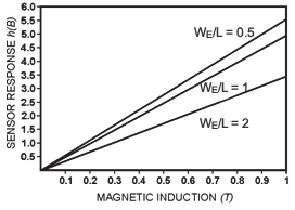
Fig. 1.2. The h(B) depending on B for three devices of different geometry
In figure 1.2 the geometry influence on hBvalues for three magnetotransistor structures
can be seen ratios W
L W
m .
E
50
E /
MGT1: W
L
, L / W G
E
0.72;
E /
0.5
MGT2: W
L , L / W G
E
0.68;
E /
1
MGT3: W
L , L / W G
E
0.46;
E /
2
Magnetic Microsensors
5
It is noticed that the response h B is maximum for W
L
structure.
Decreasing
E /
0.5
the emitter-collector distance, h B decreases with 37.5% for W L , as compared to the E
2
maximum value. The sensor response decreases with 10.7%, comparative with W
L
E /
0.5
structure if the distance between emitter and collector doubles. For the same geometry
W
L
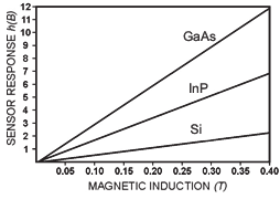
, the response is depending on material features. In figure 1.3 h B values of
E /
0.5
three sensors MGT1, MGT2, MGT3 are shown, realized on
Si (
2
1
1
0.15 m V s
),
Hn
InP (
2
1
1
0.46 m V s
)
Hn
GaAs (
2
1
1
0.80 m V s
).
Hn
Fig. 1.3. The h(B) depending on B for three devices on different materials
A magnetotransistor may be regarded as a modulation transducer that converts the
magnetic induction signal into an electric current signal.
This current signal or output signal is the variation of collector current, caused by
induction B .
The absolute sensitivity of a magnetotransistor used as magnetic sensors is:
1
L
S I
B
G I
(1.3)
A
C /
2 Hn
C
WE
The magnetic sensitivity related to the devices current is defined as follows:
1
I
L
C
1
S
G
(1.4)
I
I B
2 Hn W
C
E
For a given induction B 0,4 T and at given collector current I mA , the sensitivity C
1
depends on the device geometry and the material properties. In table 1.1 the obtained values
for five magnetotransistors structures are presented.
6
Microsensors
The analysis of the main characteristics of the double-collector magnetotransistor shows that
the W
L
structure is theoretically favourable to high performance regarding signal-
E /
0.5
to-noise ratio, as well as the offset equivalent magnetic induction. Also substituting the
silicon technology by using other materials such as GaAs or InSb with high carriers mobility
values assure higher characteristics of the sensors
W
L
2
1
1
m V s
1
S T
I [
]
Hn [
]
E /
MGT1 2
0,15
Si
0,035
MGT2 1
0,15
Si
0,05
MGT3 0,5
0,15
Si
0,055
MGT4 0,5
0,46
InP
0,168
MGT5 0,5
0,85
GaAs
0,292
Table 1.1. The numerical values of the supply-current-related sensitivity.
1.3 The offset equivalent magnetic induction
The difference between the two collector currents in the absence of the magnetic field is the
offset collector current:
I
I
I
(1.5)
C
C (0)
C (0)
1
2
off
The causes consist of imperfections specific to the manufacturing process: the contact non-
linearity, the non-uniformity of the thickness and of the epitaxial layer doping, the presence
of some mechanical stresses combined with the piezo-resistive effect.
To describe the error due to the offset the magnetic induction is determined, which
produces the imbalance I
I
. The offset equivalent magnetic induction is expressed
C
C off
by considering the relation (4):
1
I
I
Coff
2
L
Coff
B
G
(1.6)
off
S I
I
W
I C
Hn
C
E
Consid