High Performance Computing by Charles Severance - HTML preview
Download the book in PDF, ePub, Kindle for a complete version.
Chapter 2
Memory
2.1 Introduction1
2.1.1 Memory
Let's say that you are fast asleep some night and begin dreaming. In your dream, you have a time machine and a few 500-MHz four-way superscalar processors. You turn the time machine back to 1981. Once you arrive back in time, you go out and purchase an IBM PC with an Intel 8088 microprocessor running at 4.77
MHz. For much of the rest of the night, you toss and turn as you try to adapt the 500-MHz processor to the Intel 8088 socket using a soldering iron and Swiss Army knife. Just before you wake up, the new computer nally works, and you turn it on to run the Linpack2 benchmark and issue a press release. Would you expect this to turn out to be a dream or a nightmare? Chances are good that it would turn out to be a nightmare, just like the previous night where you went back to the Middle Ages and put a jet engine on a horse. (You have got to stop eating double pepperoni pizzas so late at night.)
Even if you can speed up the computational aspects of a processor innitely fast, you still must load and store the data and instructions to and from a memory. Today's processors continue to creep ever closer to innitely fast processing. Memory performance is increasing at a much slower rate (it will take longer for memory to become innitely fast). Many of the interesting problems in high performance computing use a large amount of memory. As computers are getting faster, the size of problems they tend to operate on also goes up. The trouble is that when you want to solve these problems at high speeds, you need a memory system that is large, yet at the same time fasta big challenge. Possible approaches include the following:
• Every memory system component can be made individually fast enough to respond to every memory access request.
• Slow memory can be accessed in a round-robin fashion (hopefully) to give the eect of a faster memory system.
• The memory system design can be made wide so that each transfer contains many bytes of information.
• The system can be divided into faster and slower portions and arranged so that the fast portion is used more often than the slow one.
Again, economics are the dominant force in the computer business. A cheap, statistically optimized memory system will be a better seller than a prohibitively expensive, blazingly fast one, so the rst choice is not much of a choice at all. But these choices, used in combination, can attain a good fraction of the performance you would get if every component were fast. Chances are very good that your high performance workstation incorporates several or all of them.
1This content is available online at <http://cnx.org/content/m32733/1.1/>.
2See Chapter 15, Using Published Benchmarks, for details on the Linpack benchmark.
Once the memory system has been decided upon, there are things we can do in software to see that it is used eciently. A compiler that has some knowledge of the way memory is arranged and the details of the caches can optimize their use to some extent. The other place for optimizations is in user applications, as we'll see later in the book. A good pattern of memory access will work with, rather than against, the components of the system.
In this chapter we discuss how the pieces of a memory system work. We look at how patterns of data and instruction access factor into your overall runtime, especially as CPU speeds increase. We also talk a bit about the performance implications of running in a virtual memory environment.
2.2 Memory Technology3
2.2.1 Memory Technology
Almost all fast memories used today are semiconductor-based.4 They come in two avors: dynamic random access memory (DRAM) and static random access memory (SRAM). The term random means that you can address memory locations in any order. This is to distinguish random access from serial memories, where you have to step through all intervening locations to get to the particular one you are interested in. An example of a storage medium that is not random is magnetic tape. The terms dynamic and static have to do with the technology used in the design of the memory cells. DRAMs are charge-based devices, where each bit is represented by an electrical charge stored in a very small capacitor. The charge can leak away in a short amount of time, so the system has to be continually refreshed to prevent data from being lost. The act of reading a bit in DRAM also discharges the bit, requiring that it be refreshed. It's not possible to read the memory bit in the DRAM while it's being refreshed.
SRAM is based on gates, and each bit is stored in four to six connected transistors. SRAM memories retain their data as long as they have power, without the need for any form of data refresh.
DRAM oers the best price/performance, as well as highest density of memory cells per chip. This means lower cost, less board space, less power, and less heat. On the other hand, some applications such as cache and video memory require higher speed, to which SRAM is better suited. Currently, you can choose between SRAM and DRAM at slower speeds down to about 50 nanoseconds (ns). SRAM has access times down to about 7 ns at higher cost, heat, power, and board space.
In addition to the basic technology to store a single bit of data, memory performance is limited by the practical considerations of the on-chip wiring layout and the external pins on the chip that communicate the address and data information between the memory and the processor.
2.2.1.1 Access Time
The amount of time it takes to read or write a memory location is called the memory access time. A related quantity is the memory cycle time. Whereas the access time says how quickly you can reference a memory location, cycle time describes how often you can repeat references. They sound like the same thing, but they're not. For instance, if you ask for data from DRAM chips with a 50-ns access time, it may be 100 ns before you can ask for more data from the same chips. This is because the chips must internally recover from the previous access. Also, when you are retrieving data sequentially from DRAM chips, some technologies have improved performance. On these chips, data immediately following the previously accessed data may be accessed as quickly as 10 ns.
Access and cycle times for commodity DRAMs are shorter than they were just a few years ago, meaning that it is possible to build faster memory systems. But CPU clock speeds have increased too. The home computer market makes a good study. In the early 1980s, the access time of commodity DRAM (200 ns) was shorter than the clock cycle (4.77 MHz = 210 ns) of the IBM PC XT. This meant that DRAM could 3This content is available online at <http://cnx.org/content/m32716/1.1/>. 4Magnetic core memory is still used in applications where radiation hardness resistance to changes caused by ionizing radiation is important. be connected directly to the CPU without worrying about over running the memory system. Faster XT and AT models were introduced in the mid-1980s with CPUs that clocked more quickly than the access times of available commodity memory. Faster memory was available for a price, but vendors punted by selling computers with wait states added to the memory access cycle. Wait states are articial delays that slow down references so that memory appears to match the speed of a faster CPU at a penalty. However, the technique of adding wait states begins to signicantly impact performance around 25?33MHz. Today, CPU speeds are even farther ahead of DRAM speeds.
The clock time for commodity home computers has gone from 210 ns for the XT to around 3 ns for a 300-MHz Pentium-II, but the access time for commodity DRAM has decreased disproportionately less from 200 ns to around 50 ns. Processor performance doubles every 18 months, while memory performance doubles roughly every seven years.
The CPU/memory speed gap is even larger in workstations. Some models clock at intervals as short as 1.6 ns. How do vendors make up the dierence between CPU speeds and memory speeds? The memory in the Cray-1 supercomputer used SRAM that was capable of keeping up with the 12.5-ns clock cycle. Using SRAM for its main memory system was one of the reasons that most Cray systems needed liquid cooling.
Unfortunately, it's not practical for a moderately priced system to rely exclusively on SRAM for storage.
It's also not practical to manufacture inexpensive systems with enough storage using exclusively SRAM.
The solution is a hierarchy of memories using processor registers, one to three levels of SRAM cache, DRAM main memory, and virtual memory stored on media such as disk. At each point in the memory hierarchy, tricks are employed to make the best use of the available technology. For the remainder of this chapter, we will examine the memory hierarchy and its impact on performance.
In a sense, with today's high performance microprocessor performing computations so quickly, the task of the high performance programmer becomes the careful management of the memory hierarchy. In some sense it's a useful intellectual exercise to view the simple computations such as addition and multiplication as innitely fast in order to get the programmer to focus on the impact of memory operations on the overall performance of the program.
2.3 Registers5
2.3.1 Registers
At least the top layer of the memory hierarchy, the CPU registers, operate as fast as the rest of the processor.
The goal is to keep operands in the registers as much as possible. This is especially important for intermediate values used in a long computation such as:
X = G * 2.41 + A / W - W * M
While computing the value of A divided by W, we must store the result of multiplying G by 2.41. It would be a shame to have to store this intermediate result in memory and then reload it a few instructions later.
On any modern processor with moderate optimization, the intermediate result is stored in a register. Also, the value W is used in two computations, and so it can be loaded once and used twice to eliminate a wasted load.Compilers have been very good at detecting these types of optimizations and eciently making use of the available registers since the 1970s. Adding more registers to the processor has some performance benet.
It's not practical to add enough registers to the processor to store the entire problem data. So we must still use the slower memory technology.
5This content is available online at <http://cnx.org/content/m32681/1.1/>.
2.4 Caches6
2.4.1 Caches
Once we go beyond the registers in the memory hierarchy, we encounter caches. Caches are small amounts of SRAM that store a subset of the contents of the memory. The hope is that the cache will have the right subset of main memory at the right time.
The actual cache architecture has had to change as the cycle time of the processors has improved. The processors are so fast that o-chip SRAM chips are not even fast enough. This has lead to a multilevel cache approach with one, or even two, levels of cache implemented as part of the processor.
Table 2.1 shows the approximate speed of accessing the memory hierarchy on a 500-MHz DEC 21164 Alpha.
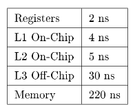
Table 2.1: Table 3-1: Memory Access Speed on a DEC 21164 Alpha
When every reference can be found in a cache, you say that you have a 100% hit rate. Generally, a hit rate of 90% or better is considered good for a level-one (L1) cache. In level-two (L2) cache, a hit rate of above 50% is considered acceptable. Below that, application performance can drop o steeply.
One can characterize the average read performance of the memory hierarchy by examining the probability that a particular load will be satised at a particular level of the hierarchy. For example, assume a memory architecture with an L1 cache speed of 10 ns, L2 speed of 30 ns, and memory speed of 300 ns. If a memory reference were satised from L1 cache 75% of the time, L2 cache 20% of the time, and main memory 5% of the time, the average memory performance would be:
(0.75 * 10 ) + ( 0.20 * 30 ) + ( 0.05 * 300 ) = 28.5 ns
You can easily see why it's important to have an L1 cache hit rate of 90% or higher.
Given that a cache holds only a subset of the main memory at any time, it's important to keep an index of which areas of the main memory are currently stored in the cache. To reduce the amount of space that must be dedicated to tracking which memory areas are in cache, the cache is divided into a number of equal sized slots known as lines. Each line contains some number of sequential main memory locations, generally four to sixteen integers or real numbers. Whereas the data within a line comes from the same part of memory, other lines can contain data that is far separated within your program, or perhaps data from somebody else's program, as in Figure 2.1 (Figure 3-1: Cache lines can come from dierent parts of memory). When you ask for something from memory, the computer checks to see if the data is available within one of these cache lines. If it is, the data is returned with a minimal delay. If it's not, your program may be delayed while a new line is fetched from main memory. Of course, if a new line is brought in, another has to be thrown out.
If you're lucky, it won't be the one containing the data you are just about to need.
6This content is available online at <http://cnx.org/content/m32725/1.1/>.
Figure 3-1: Cache lines can come from dierent parts of memory
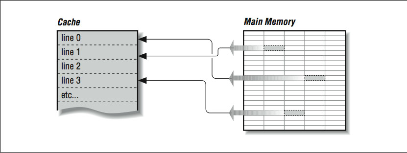
Figure 2.1
On multiprocessors (computers with several CPUs), written data must be returned to main memory so the rest of the processors can see it, or all other processors must be made aware of local cache activity.
Perhaps they need to be told to invalidate old lines containing the previous value of the written variable so that they don't accidentally use stale data. This is known as maintaining coherency between the dierent caches. The problem can become very complex in a multiprocessor system.7
Caches are eective because programs often exhibit characteristics that help kep the hit rate high. These characteristics are called spatial and temporal locality of reference; programs often make use of instructions and data that are near to other instructions and data, both in space and time. When a cache line is retrieved from main memory, it contains not only the information that caused the cache miss, but also some neighboring information. Chances are good that the next time your program needs data, it will be in the cache line just fetched or another one recently fetched.
Caches work best when a program is reading sequentially through the memory. Assume a program is reading 32-bit integers with a cache line size of 256 bits. When the program references the rst word in the cache line, it waits while the cache line is loaded from main memory. Then the next seven references to memory are satised quickly from the cache. This is called unit stride because the address of each successive data element is incremented by one and all the data retrieved into the cache is used. The following loop is a unit-stride loop:
DO I=1,1000000
SUM = SUM + A(I)
END DO
When a program accesses a large data structure using non-unit stride, performance suers because data is loaded into cache that is not used. For example:
7Chapter 10, Shared-Memory Multiprocessors, describes cache coherency in more detail.
DO I=1,1000000, 8
SUM = SUM + A(I)
END DO
This code would experience the same number of cache misses as the previous loop, and the same amount of data would be loaded into the cache. However, the program needs only one of the eight 32-bit words loaded into cache. Even though this program performs one-eighth the additions of the previous loop, its elapsed time is roughly the same as the previous loop because the memory operations dominate performance.
While this example may seem a bit contrived, there are several situations in which non-unit strides occur quite often. First, when a FORTRAN two-dimensional array is stored in memory, successive elements in the rst column are stored sequentially followed by the elements of the second column. If the array is processed with the row iteration as the inner loop, it produces a unit-stride reference pattern as follows:
REAL*4 A(200,200)
DO J = 1,200
DO I = 1,200
SUM = SUM + A(I,J)
END DO
END DO
Interestingly, a FORTRAN programmer would most likely write the loop (in alphabetical order) as follows, producing a non-unit stride of 800 bytes between successive load operations:
REAL*4 A(200,200)
DO I = 1,200
DO J = 1,200
SUM = SUM + A(I,J)
END DO
END DO
Because of this, some compilers can detect this suboptimal loop order and reverse the order of the loops to make best use of the memory system. As we will see in Chapter 4, however, this code transformation may produce dierent results, and so you may have to give the compiler permission to interchange these loops in this particular example (or, after reading this book, you could just code it properly in the rst place). while ( ptr != NULL ) ptr = ptr->next;
The next element that is retrieved is based on the contents of the current element. This type of loop bounces all around memory in no particular pattern. This is called pointer chasing and there are no good ways to improve the performance of this code.
A third pattern often found in certain types of codes is called gather (or scatter) and occurs in loops such as:
SUM = SUM + ARR ( IND(I) )
where the IND array contains osets into the ARR array. Again, like the linked list, the exact pattern of memory references is known only at runtime when the values stored in the IND array are known. Some special-purpose systems have special hardware support to accelerate this particular operation.
2.5 Cache Organization8
2.5.1 Cache Organization
The process of pairing memory locations with cache lines is called mapping. Of course, given that a cache is smaller than main memory, you have to share the same cache lines for dierent memory locations. In caches, each cache line has a record of the memory address (called the tag) it represents and perhaps when it was last used. The tag is used to track which area of memory is stored in a particular cache line.
The way memory locations (tags) are mapped to cache lines can have a benecial eect on the way your program runs, because if two heavily used memory locations map onto the same cache line, the miss rate will be higher than you would like it to be. Caches can be organized in one of several ways: direct mapped, fully associative, and set associative.
2.5.1.1 Direct-Mapped Cache
Direct mapping, as shown in Figure 2.2 (Figure 3-2: Many memory addresses map to the same cache line), is the simplest algorithm for deciding how memory maps onto the cache. Say, for example, that your computer has a 4-KB cache. In a direct mapped scheme, memory location 0 maps into cache location 0, as do memory locations 4K, 8K, 12K, etc. In other words, memory maps onto the cache size. Another way to think about it is to imagine a metal spring with a chalk line marked down the side. Every time around the spring, you encounter the chalk line at the same place modulo the circumference of the spring. If the spring is very long, the chalk line crosses many coils, the analog being a large memory with many locations mapping into the same cache line.
Problems occur when alternating runtime memory references in a direct-mapped cache point to the same cache line. Each reference causes a cache miss and replaces the entry just replaced, causing a lot of overhead.
The popular word for this is thrashing. When there is lots of thrashing, a cache can be more of a liability than an asset because each cache miss requires that a cache line be relled an operation that moves more data than merely satisfying the reference directly from main memory. It is easy to construct a pathological case that causes thrashing in a 4-KB direct-mapped cache:
8This content is available online at <http://cnx.org/content/m32722/1.1/>.
Figure 3-2: Many memory addresses map to the same cache line
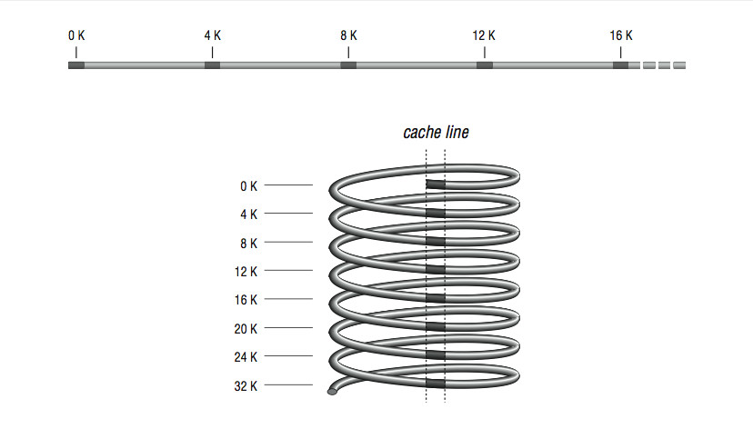
Figure 2.2
REAL*4 A(1024), B(1024)
COMMON /STUFF/ A,B
DO I=1,1024
A(I) = A(I) * B(I)
END DO
END
The arrays A and B both take up exactly 4 KB of storage, and their inclusion together in COMMON assures that the arrays start exactly 4 KB apart in memory. In a 4-KB direct mapped cache, the same line that is used for A(1) is used for B(1), and likewise for A(2) and B(2), etc., so alternating references cause repeated cache misses. To x it, you could either adjust the size of the array A, or put some other variables into COMMON, between them. For this reason one should generally avoid array dimensions that are close to powers of two.
2.5.1.2 Fully Associative Cache
At the other extreme from a direct mapped cache is a fully associative cache, where any memory location can be mapped into any cache line, regardless of memory address. Fully associative caches get their name from the type of memory used to construct them associative memory. Associative memory is like regular memory, except that each memory cell knows something about the data it contains.
When the processor goes looking for a piece of data, the cache lines are asked all at once whether any of them has it. The cache line containing the data holds up its hand and says I have it; if none of them do, there is a cache miss. It then becomes a question of which cache line will be replaced with the new data.
Rather than map memory locations to cache lines via an algorithm, like a direct- mapped cache, the memory system can ask the fully associative cache lines to choose among themselves which memory locations they will represent. Usually the least recently used line is the one that gets overwritten with new data. The assumption is that if the data hasn't been used in quite a while, it is least likely to be used in the future.
Fully associative caches have superior utilization when compared to direct mapped caches. It's dicult to nd real-world examples of programs that will cause thrashing in a fully associative cache. The expense of fully associative caches is very high, in terms of size, price, and speed. The associative caches that do exist tend to be small.
2.5.1.3 Set-Associative Cache
Now imagine that you have two direct mapped caches sitting side by side in a single cache unit as shown in Figure 2.3 (Figure 3-3: Two-way set-associative cache). Each memory location corresponds to a particular cache line in each of the two direct-mapped caches. The one you choose to replace during a cache miss is subject to a decision about whose line was used last the same way the decision was made in a fully associative cache except that now there are only two choices. This is called a set-associative cache. Set-associative caches generally come in two and four separate banks of cache. These are called two-way and four-way set associative caches, respectively. Of course, there are benets and drawbacks to each type of cache. A set-associative cache is more immune to cache thrashing than a direct-mapped cache of the same size, because for each mapping of a memory address into a cache line, there are two or more choices where it can go. The beauty of a direct-mapped cache, however, is that it's easy to implement and, if made large enough, will perform roughly as well as a set-associative design. Your machine may contain multiple caches for several dierent purposes. Here's a little program for causing thrashing in a 4-KB two-way set- associative cache:
REAL*4 A(1024), B(1024), C(1024)
COMMON /STUFF/ A,B,C
DO I=1,1024
A(I) = A(I) * B(I) + C(I)
END DO
END
Like the previous cache thrasher program, this forces repeated accesses to the same cache lines, except that now there are three variables contending for the choose set same mapping instead of two. Again, the way to x it would be to change the size of the arrays or insert something in between them, in COMMON. By the way, if you accidentally arranged a program to thrash like this, it would be hard for you to detect it aside from a feeling that the program runs a little slow. Few vendors provide tools for measuring cache misses.
Figure 3-3: Two-way set-associative cache
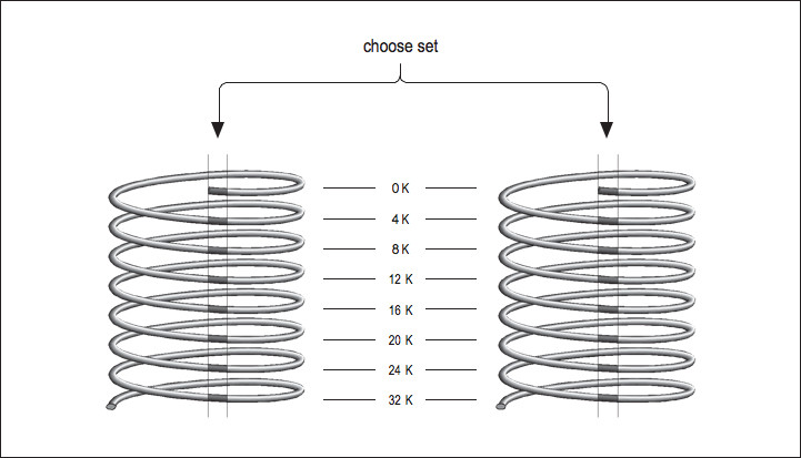
Figure 2.3
2.5.1.4 Instruction Cache
So far we have glossed over the two kinds of information you would expect to nd in a cache between main memory and the CPU: instructions and data. But if you think about it, the demand for data is separate from the demand for instructions. In superscalar processors, for example, it's possible to execute an instruction that causes a data cache miss alongside other instructions that require no data from cache at all, i.e., they operate on registers. It doesn't seem fair that a cache miss on a data reference in one instruction should keep you from fetching other instructions because the cache is tied up. Furthermore, a cache depends on locality of reference between bits of data and other bits of data or instructions and other instructions, but what kind of interplay is there between instructions and data? It would seem possible for instructions to bump perfectly useful data from cache, or vice versa, with complete disregard for locality of reference.
Many designs from the 1980s used a single cache for both instructions and data. But newer designs are employing what is known as the Harvard Memory Architecture, where the demand for data is segregated from the demand for instructions.
Main memory is a still a single large pool, but these processors have separate data and instruction caches, possibly of dierent designs. By providing two independent sources for data and instructions, the aggregate rate of information coming from memory is increased, and interference between the two types of memory references is minimized. Also, instructions generally have an extremely high level of locality of reference because of the sequential nature of most programs. Because the instruction caches don't have to be particularly large to be eective, a typical architecture is to have separate L1 caches for instructions and data and to have a combined L2 cache. For example, the IBM/Motorola PowerPC 604e has separate 32-K four-way set-associative L1 caches for instruction and data and a combined L2 cache.
2.6 Virtual Memory9
2.6.1 Virtual Memory
Virtual memory decouples the addresses used by the program (virtual addresses) from the actual addresses where the data is stored in memory (physical addresses). Your program sees its address space starting at 0 and working its way up to some large number, but the actual physical addresses assigned can be very dierent. It gives a degree of exibility by allowing all processes to believe they have the entire memory system to themselves. Another trait of virtual memory systems is that they divide your program's memory up into pages chunks. Page sizes vary from 512 bytes to 1 MB or larger, depending on the machine. Pages don't have to be allocated contiguously, though your program sees them that way. By being separated into pages, programs are easier to arrange in memory, or move portions out to disk.
2.6.1.1 Page Tables
Say that your program asks for a variable stored at location 1000. In a virtual memory machine, there is no direct correspondence between your program's idea of where location 1000 is and the physical memory systems' idea. To nd where your variable is actually stored, the location has to be translated from a virtual to a physical address. The map containing such translations is called a page table. Each process has a several page tables associated with it, corresponding to dierent regions, such as program text and data segments.
To understand how address translation works, imagine the following scenario: at some point, your pro– gram asks for data from location 1000. Figure 2.4 (Figure 3-4: Virtual-to-physical address mapping) shows the steps required to complete the retrieval of this data. By choosing location 1000, you have identied which region the memory reference falls in, and this identies which page table is involved. Location 1000 then helps the processor choose an entry within the table. For instance, if the page size is 512 bytes, 1000 falls within the second page (pages range from addresses 0511, 5121023, 10241535, etc.).
Therefore, the second table entry should hold the address of the page housing the value at location 1000.
9This content is available online at <http://cnx.org/content/m32728/1.1/>.
Figure 3-4: Virtual-to-physical address mapping
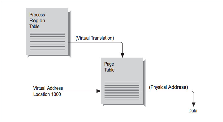
Figure 2.4
The operating system stores the page-table addresses virtually, so it's going to take a virtual-to-physical translation to locate the table in memory. One more virtual-to- physical translation, and we nally have the true address of location 1000. The memory reference can complete, and the processor can return to executing your program.
2.6.1.2 Translation Lookaside Buer
As you can see, address translation through a page table is pretty complicated. It required two table lookups (maybe three) to locate our data. If e