Electronics Module by Sam Kinyera OBWOYA - HTML preview
Download the book in PDF, ePub, Kindle for a complete version.
v
m
Vi
Numerical Example
A field effect transistor having g = 4 mA/ V and =60
m
rd
kΩ is used with a drain
load resistance of 30 kΩ in a.f. voltage amplifier. Find the voltage gain.
Solution
r R
30 × 60
R = d D =
= 20 kΩ
r + R
30 + 60
d
D
A = g R = 4 × 20 = 80
v
m


African Virtual University
Task 2.5 Note making and further reading
Use the references and make notes on
i. Output and output phase relation
ii. Gate biasing
iii. Load line calculations
Activity 2.2.5
MOSFET
1. Structure
(i) MOSFET is a form of FET where the gate is insulated from the channel by a
thin layer of silicon oxide as shown in Fig. 2.17.
(ii) Accordingly, in a MOSFET,
-
no leakage of current between gate and channel occurs and
-
the input resistance is of hundreds of megohms.
S
G
D
Silicon oxide
N-channel
P-substrate
Base
Figure 2.17 Construction of MOSFET (depletion type)
Note that the gate is coupled by capacitance effect through the oxide and channel.
When gate is provided with positive bias, a field is set up through the oxide which
attracts electrons to the gate region. This conduction takes place between source and
drain. The degree of conduction depends on how positive the gate is with respect
to source.
• For: n-channel MOSFET output characteristics see: http://jas.eng.buffalo.
edu/education/transistor/n_MOS_IV/mosfet.html. 10 th August 2007.

African Virtual University 0
Task 2.6 Note making and further reading
Use the references and complete the notes on:
- output characteristics curves when the magnitude of positive bias in MOSFET
is varied
Self Evaluation 2
1. Carry out the analysis of CE and show thatα = 1 / 1
( + β).
Hint: Write the relation for β in terms of collector and base currents first.
dc
2. Show that in a CC configuration
Output current = 1
( + β)× input current
3. With reference to a transistor
(
α I
I
a) Show that I
B
CBO
=
C
1
(
) + 1( ) and
− α
− α
(b)Similarly, show that I (
)I
= 1− α
− I
B
E
CBO
(c)Repeat activity 2.1.7 for CE Circuit

African Virtual University
Activity 3: Operational Amplifiers
You will require 10 hours to complete this activity. Only basic guidelines are provided
to help you go through the activity.
Specific Teaching and Learning Objectives
In this activity you will be required to:
i. Explain the construction of operational amplifier, and
ii. Design, analyse and synthesize operational amplifier circuits.
Summary of the learning activity
The activity involves learning about the general features of an operational amplifier,
the principles behind its operation and its applications in classical computation which
include addition, subtraction, multiplication, division, integration and differentiation.
Relevant equations are derived and used to solve numerical problems.
List of REQUIRED readings
Reading 1: Electronics WIKIBOOKS
Reference: http://en.wikibooks.org/wiki/Electronics. 5th October 2007.
Abstract: Topics covered in this reading include: Analogue circuits, Digital circuits,
Elements of Digital Circuits, Computer architecture, Analogue-to-Digital and Digital-
to-Analogue converters.
Rationale: The reading adequately covers the basic course of electronics outline
in the activity.
Reading 2: Operational Amplifier WIKIBOOKS
Reference: http://en.wikibooks.org/wiki/Electronics/Op-Amp. 5th October 2007.
Abstract: Reading 3 include: Amplifiers, op-amp, notation, quick design process,
ideal op-amps, basic op-amps configuration, advanced op-amp configurations and
real op-amp.
Rationale: This provides most of the required reading on operational amplifier that
is needed for the course.

African Virtual University
List of relevant MULTIMEDIA resources
Reference: http://server.oersted.dtu.dk/personal/ldn/javalab/Circuit03.html. 3rd
October 2007.
Summary: This resource is on inverting amplifier where the voltage source is turned
on in order to check the circuit for different values of the resistances and/or the open-
loop gain of the opamp.
Rationale: In the (normal) case of a large open-loop gain of the opamp (typically
>100 dB) the feedback mechanism will force the inverting input terminal to be virtu-
ally grounded. In this limit the closed-loop amplification factor of the circuit will be
determined solely by the resistance values.
List of Relevant Useful Links
Title: Operational amplifier.
URL: http://ocw.mit.edu/OcwWeb/Electrical-Engineering-and-Computer-Science/6-
002Circuits-and-ElectronicsFall2000/VideoLectures/index.htm. 3rd October 2007.
Abstact: These contain course lecture slides accompanying video lectures, and de-
scriptions of live demonstration shown by instructor during lectures.
Title: OP-Amps.
URL: http://en.wikibooks.org/wiki/Electronics/Op-Amps”. 4th October 2007.
Abstract: Provides good reading materials on amplifiers, Op-Amp, notation, ideal
Op-Amps, basic Op-Amp configurations, and real Op-Amp.
Title: Operational Amplifier.
URL:http://en.wikipedia.org/wiki/Operational_amplifier. 4th October 2007.
Abstract: This has good reading materials on operational amplifier. The topics in-
clude: basic operation, the ideal op-amp, limitations of real op-amps, notations, use of
electronics system design, DC behaviour, AC behaviour, Basic non-inverting amplifier
circuit, internal circuitry of 741 type of op-amp, and common applications.

African Virtual University
Activity 3.1 Construction of operational amplifier
Using references like: “http://en.wikipedia.org/wiki/Operational_amplifier 6th August
2007.
You will learn that Operational amplifier:
(i) is usually abbreviated as an op-amp, and its usual circuit symbol is shown in
Fig. 3.1
(ii) has two inputs and one output, where the inputs are assumed to have very high
impedance and therefore negligible current flows into or out of the inputs.
(iii) has output which is controlled by a negative feedback in ordinary usage.
(iv) has an output voltage of an input is determined by the negative feedback
because of the amplifier’s high gain.
(v) has ideally an output impedance of zero. This means that an op-amp can
deliver an infinitely large current to the load or circuit connected to it.
(vi) Makes all classical computation possible including addition, subtraction,
multiplication, division, integration and differentiation.
VS +
where:
d
V : non-inverting input
+
V : inverting input
V
−
V
out
d
+
V : output
+
out
d
V
V : positive power supply
+
_
S+
V
(sometimes also V , V , or V
)
−
d
DD
CC
CC +
V
V : negative power supply
_
S−
(sometimes also V , V , or V
)
SS
EE
CC −
d VS−
V S _
Figure 3.1 Circuit symbol for an op-amp


African Virtual University
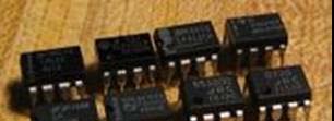
The commonest type of op-amp is the “741”. It has 8 pins. Fig. 3.2 gives their phy-
sical appearance.
Figure 3.2 Typical physical appearance of 741 Op-amp
Activity 3.2
Basic non-inverting amplifier circuit
In this activity you will learn that :
The output voltage is the difference between the + and - inputs multiplied by the
open-loop gain:V
= V
( −V )* A .
out
+
−
vo
+
V
+
in
V
+
V
V
out
_
out
in
(a)Inverting amplifier
(b)Non-inverting amplifier
Figure 3.3 Basic inverting and non-inverting amplifier circuits
(i) If an op-amp is connected as in Fig. 3.3 (a) and(b) , the ratio of
/ V
Vout
in
would be very high. This is called open-loop gain. When an Op-amp is ope-
rated without connecting any resistor or capacitor from its output to any one
of its input (i.e., without feedback), it is said to be in the open-loop condition.
The word “open loop” means that the feedback path or loop is open.

African Virtual University
(ii) In a non-inverting arrangement, the output, V , is in phase with the input
0
voltage and is an exact amplified copy of the input, but
(iii) In this case of inverting arrangement, the output voltage is exactly opposite,
amplified copy of input voltage i.e. output voltage is 180 degrees out of phase
with input voltage.
Task 3.1 Further reading and note making
Use the following references:
1. “http://en.wikipedia.org/wiki/Operational_amplifier. 12 August 2007.
2. B.L Theraja and R.S. Sedha: “Principles of Electronic devices and circuits”
a. Make complete notes about non-inverting amplifier circuit
b. State the two “golden rules” as you make the note.
c. Make notes on the difference between open loop gain and closed loop gain
For simulation of an inverting amplifier see
http://server.oersted.dtu.dk/personal/ldn/javalab/Circuit03.html. 7th July 2007
http://www.ngsir.netfirms.com/englishhtm/Amplifier.htm
http://server.oersted.dtu.dk/personal/ldn/javalab/Circuit03.html
Activity 3.2.1 Negative Feedback
R
2
+
R
1
V
_
x
out
V
in
R
3
Figure 3.4 Negative Feedback

African Virtual University
Negative feedback occurs when a little of the output signal is fed back to the inverting
input using circuit arrangement in Fig. 3.4. Since V is 180
0
0 out of phase with input,
the feedback reduces the signal the amplifier has to amplify and therefore reduces
the gain. The amount of output fed back is controlled by R .2
Some of the advantages in using negative feedback are:
1. Amplifiers with almost infinitely variable gain can be produced using one
standard Op amp circuit
2. The use of negative feedback improves the range of frequencies that the am-
plifier will amplify and improve stability.
Some OP amp characteristics
(i) There is a very high impedance between the + and the – input and ground.
Idealy this impedance is infinite but in practice it is approximately 2 MΩ .
This ensures that no current flows into the amplifier input terminals
(ii) There is zero output impedance which ensures that the amplifier is unaffected
by load
Short note
Due to the high open loop gain, a slight difference between + and – input voltages
makes the output go to its highest value which is the voltage of the supply. This is
called the saturation value, V as the output can go no higher.
s
If the voltage supply is 15V and the open loop gain is 105 then the difference in voltage
of 15/105 =150 μV produces saturation. With a V any small difference in voltage,
0
V can swing from +15 V to -15 V or the other way.
0
NB. Sketch the variation of V with for this observation
0
Vin
For the amplifier to be of any use, the – input must be at virtually the same voltage as
the + input. In the inverter amplifier circuit the + input is connected to earth which
is also 0 V, so the – input must be always virtually at the same voltage. The – input
is known as a virtual earth

African Virtual University
Activity 3.2.2 Gain of Inverting Amplifier
In Fig. 3.3 the input is kept balanced as far as possible if resistor R = R + R is
3
1
2
connected between + input and 0V, in parallel to
& R .
R1
2
Since the + input is at earth potential (virtual earth) the current through R will be
1
V / R and the current through
= V / R .
in
1
R2
0
2
Since the input impedance is very high, no current can flow into the – input. Therefore
the sum of currents at junction X must equal to zero. i.e.
V / R +V / R = 0
in
1
0
2
⇒ V / R = −V / R
in
1
0
2
(3.1)
But
V / V = −R / R = Gain
0
in
2
1
So gain of this inverting amplifier = −R / R . The minus sign indicates that the output
2
1
is inverted. The gain depends on R & R . This means that the gain is not affected by
1
2
any changes that may take place inside the op-amp, such as a change in gain due to
temperature change. So the negative feedback provides stability.
Task 3.2 Further reading and note making
Use the references and make notes on
1. Gain of non-inverting Amplifiers.
2. Voltage follower.
3. Frequency Response of op-amp Circuit.


African Virtual University
Activity 3.2.3 Gain of non-inverting Amplifier
Using Fig. 3.4, the gain of non-inverting amplifier is derived as follows.
Figure 3.5 Gain of non-inverting Amplifier
The input is applied to the + input, but the feedback is applied to the – input as shown
in Fig. 3.5. The fraction of the output signal to be fed back to the input is determined
by the potential divider R & R .
1
2 .
Let the fraction of V sent to the inverting (-) input isV , where
0
f
V × R
V =
0
1
f
(R
)
(3.2)
+ R
1
2
Let the voltage difference between the two inputs be
where
.
VT
V
.
= V − V
T
in
f
(3.3)
In this case, V is the voltage amplified i.e.
T
V = A × V .
0
0
T
(3.4)
A is the open-loop gain. Thus, substituting for in Eq. (3.3) using Eq. (3.4) we get
0
VT
V − V = A × V
in
f
0
T
(3.5)
and
V = V − V / A .
f
in
0
0
(3.6)
Again, substituting for V in Eq. (3.2) using Eq. (3.6) we have
f

African Virtual University
V
V × R
V − 0 =
0
1
in
A
(R
)
+ R
0
1
2
⎛
R
1 ⎞
∴V = V
1
+
in
0 ⎝⎜ R
A
+ R
1
2
0 ⎠
⎟
V
R + R
∴Gain = 0 = 1
2
(3.7)
A
R
1
1
1
Since A ; 105 ⇒
; 0
0
A
0
From Eq. 3.7, gain depends on R &R .
1
2
Example
Calculate the output voltage in a noninverting amplifier for an input of 120 μV if R 1
= 2.4 k Ω and R = 240kΩ .
2
Solution
The gain of an op-amp circuit is given by
R
240
A = 1+ 2 = 1+
= 101
R
2.4
1
The output voltage is then
V = AV = 101× 120μV = 12.12mV .
0
1

African Virtual University 0
Activity 3.2.4
Op-amps as summing amplifier
An op-amp is used in audio pre-amplifiers and mixers. When used to add any number